Semiconductor flash device

a technology of magnetic field and flash device, which is applied in the direction of magnetic field device, transistor, electrical apparatus, etc., can solve the problems of unfavorable device expansion and limited conventional technology, and achieve the effect of reducing the size of the device, increasing the device area, and reducing the cost of operation

Inactive Publication Date: 2006-10-26
TAIWAN SEMICON MFG CO LTD
View PDF4 Cites 244 Cited by
  • Summary
  • Abstract
  • Description
  • Claims
  • Application Information

AI Technical Summary

Problems solved by technology

The conventional technology is limited by the ability of the floating polysilicon gate to store charge.
An increase in device area i

Method used


Image

  • Semiconductor flash device
  • Semiconductor flash device
  • Semiconductor flash device

Examples


Embodiment Construction

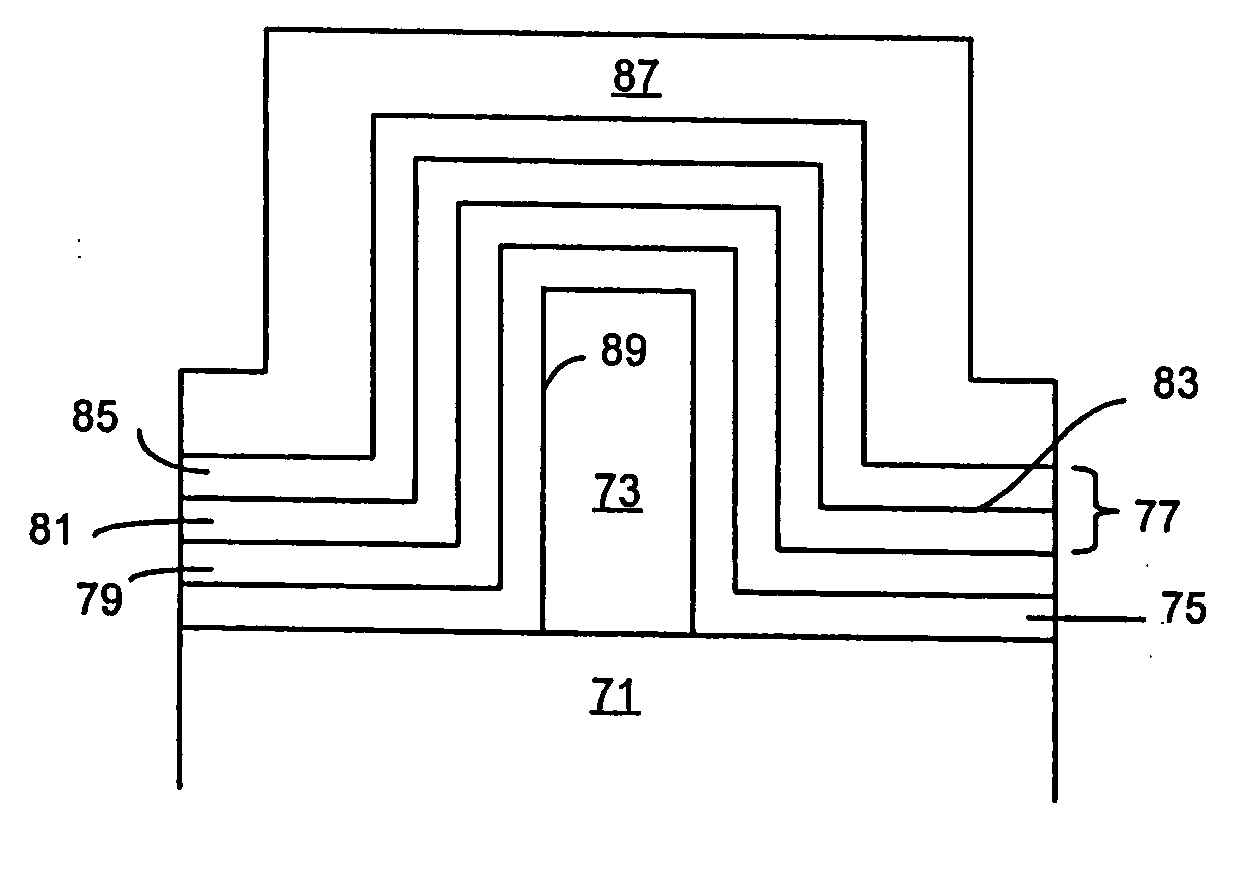
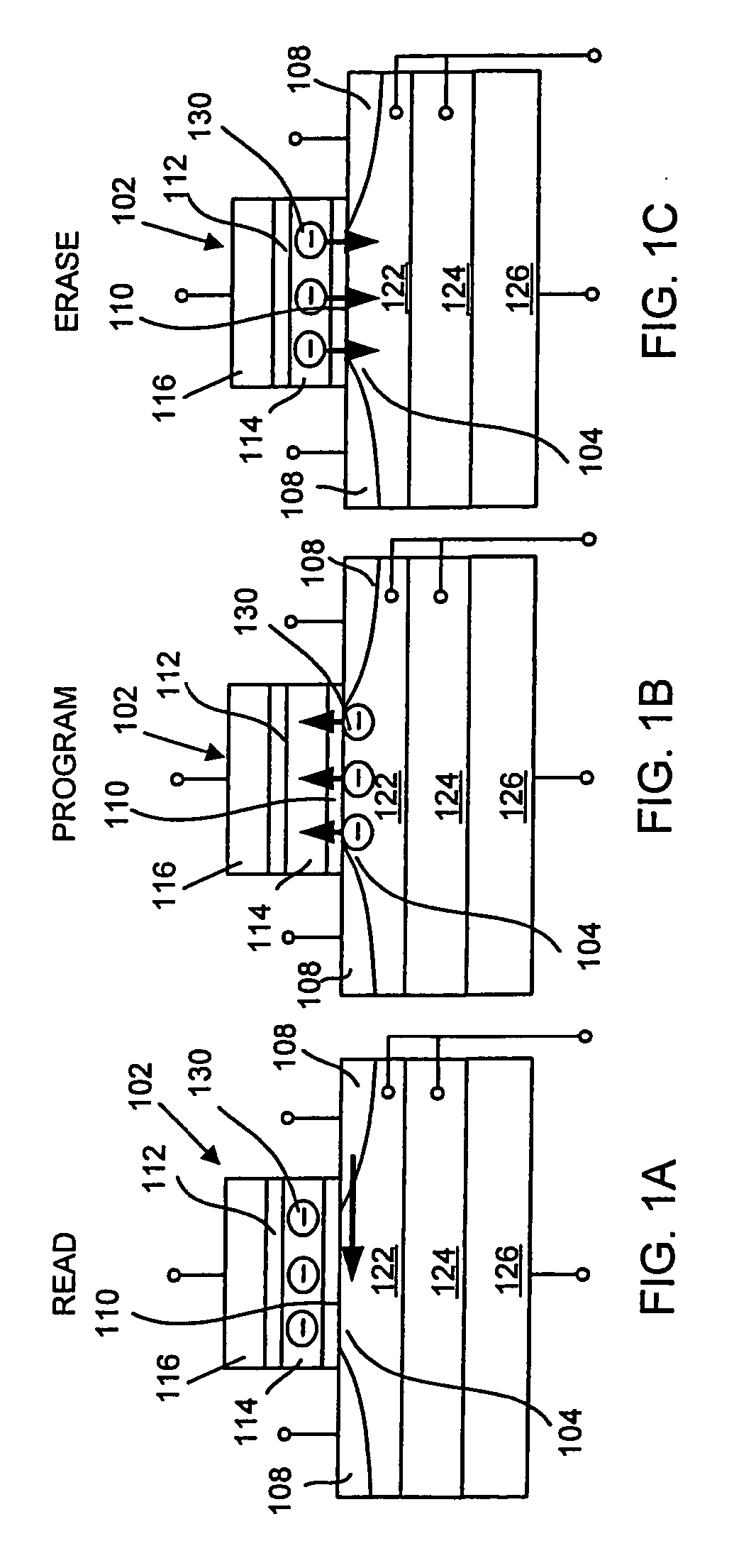
[0016] The present invention provides a floating gate transistor which may be an ETox™ or other flash memory cell with a multi-layer floating gate that includes a quantum well for superior charge retention. A thin hetero-pn junction formed between two semiconductor layers may form the quantum well due to band edge offset. The two layers are formed of materials chosen to have different bandgaps. The quantum well confines charge therein and the storage of charge in the quantum well is used to identify the logic state of the device. The thin hetero-pn junction may be lightly doped with n- and p-type dopants respectively, so that it is fully depleted of mobile carriers. The charge trapped inside the quantum well and the fully depleted multi-layer structure leads to superior charge retention of the cell and provides for further scaling down dimensions of the tunnel-oxide and channel length and enables low voltage program / erase operations. For example, as a result of this superior retenti...


PUM


Abstract

A flash memory device includes a floating gate made of a multi-layered structure. The floating gate includes a hetero-pn junction which serves as a quantum well to store charge in the floating gate, thus increasing the efficiency of the device, allowing the device to be operable using lower voltages and increasing the miniaturization of the device. The floating gate may be used in n-type and p-type devices, including n-type and p-type fin-FET devices. The stored charge may be electrons or holes.

Description

FIELD OF THE INVENTION [0001] The present invention relates most generally to semiconductor devices and more particularly to floating gate charge storage devices such as transistors. BACKGROUND [0002] Floating gate transistors are widely used in semiconductor manufacturing because of their ability to store charge in the floating gate disposed between lower and upper dielectrics formed beneath the gate electrode. Floating gate transistors are used to form flash memory cell structures such as discussed in K. Kim and G. Koh, “Future Memory Technology Including Emerging New Memories”, Intl. Conf. on Microelectronics, p. 377-384, 2004, and G. Atwood, “Future Directions and Challenges for ETox™ Flash Memory Scaling”, IEEE Trans. Device and Materials Reliability vol. 4, no. 3, September 2004. Such cell structures typically use a dual-poly floating gate structure with the polysilicon floating gate serving as a charge storage medium as shown in FIGS. 1A-1C. The tunnel-oxide of such devices i...

Claims


Application Information

Patent Timeline
IPC IPC(8): H01L29/788
CPCH01L29/7881H01L29/42324
Inventor HUANG, CHIEN-CHAOMIN-HWA, CHIYANG, FU-LIANG
Owner TAIWAN SEMICON MFG CO LTD
Why Eureka
Try Eureka