Radio frequency identification tag with improved directivity and coverage distance stability

a radio frequency identification and directivity technology, applied in the field of radio frequency identification tags, can solve the problems of remarkable drop in coverage distance or communication distance, inability to communicate in some cases, etc., and achieve the effect of wide directivity, free from the drop of communication distance, and rich flexibility

Inactive Publication Date: 2006-11-02
HITACHI LTD
View PDF17 Cites 36 Cited by
  • Summary
  • Abstract
  • Description
  • Claims
  • Application Information

AI Technical Summary

Benefits of technology

[0011] In view of the problems described above, the invention is directed to provide a radio frequency IC tag that has wide directivity, is free from the drop of the communication distance even when used for a metal and an article containing moisture and is rich in flexibility.

Problems solved by technology

However, the coverage distance or communication distance remarkably drops and communication cannot be made in some cases according to the dipole antenna having the construction shown in FIG. 14 when the material of an article to which the radio frequency IC tag is fitted is a metal or a material containing moisture such as a tree, a meat, a living body, a vegetable, and so forth.

Method used


Image

  • Radio frequency identification tag with improved directivity and coverage distance stability
  • Radio frequency identification tag with improved directivity and coverage distance stability
  • Radio frequency identification tag with improved directivity and coverage distance stability

Examples


first embodiment

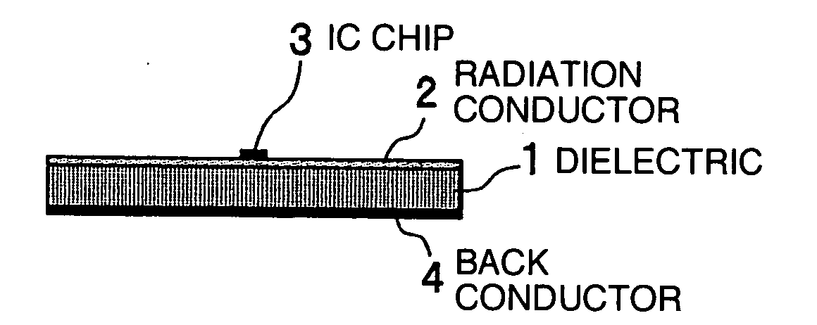
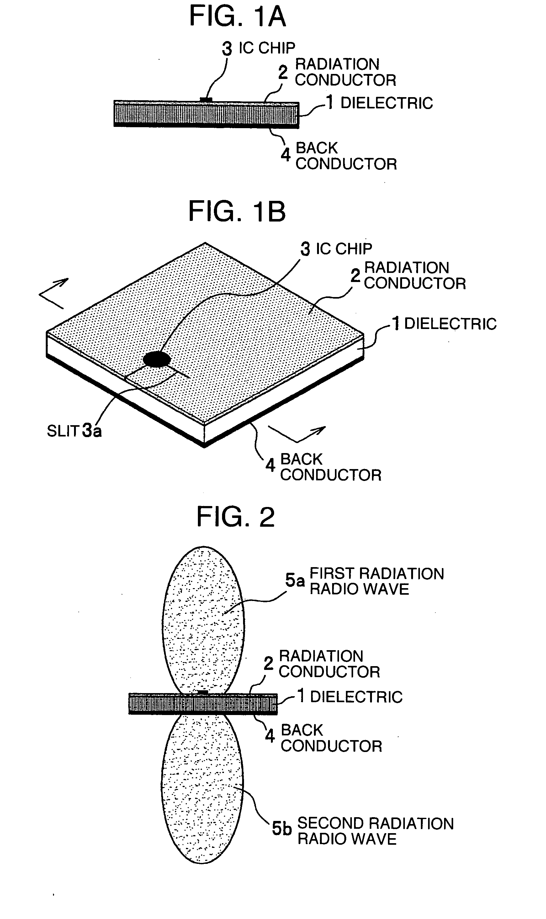
[0036]FIGS. 1A and 1B show a micro-strip antenna of a radio wave IC tag according to the first embodiment of the invention. FIG. 1A is a sectional view and FIG. 1B is a perspective view. A radiation conductor 2 is formed on the entire front surface of a dielectric 1 and a back conductor 4 is formed on the entire back surface of the dielectric 1. An IC chip 3 is mounted to a position deviated from the center of the radiation conductor 2 on the front surface side. An L-shaped slit 3a is formed at the portion of the radiation conductor 2 at which the IC chip 3 is mounted. One of the ends of the slit 3a extends to one of the ends of the radiation conductor 2 as shown in the drawing. Each bonding pad (not shown in the drawing) of the IC chip 3 is connected to the radiation conductor 2 on both sides of the slit 3a in such a fashion as to bridging the slit 3a. This slit 3a is formed to prevent dielectric breakdown and to establish impedance matching.

[0037] The dielectric 1 sandwiched betw...

second embodiment

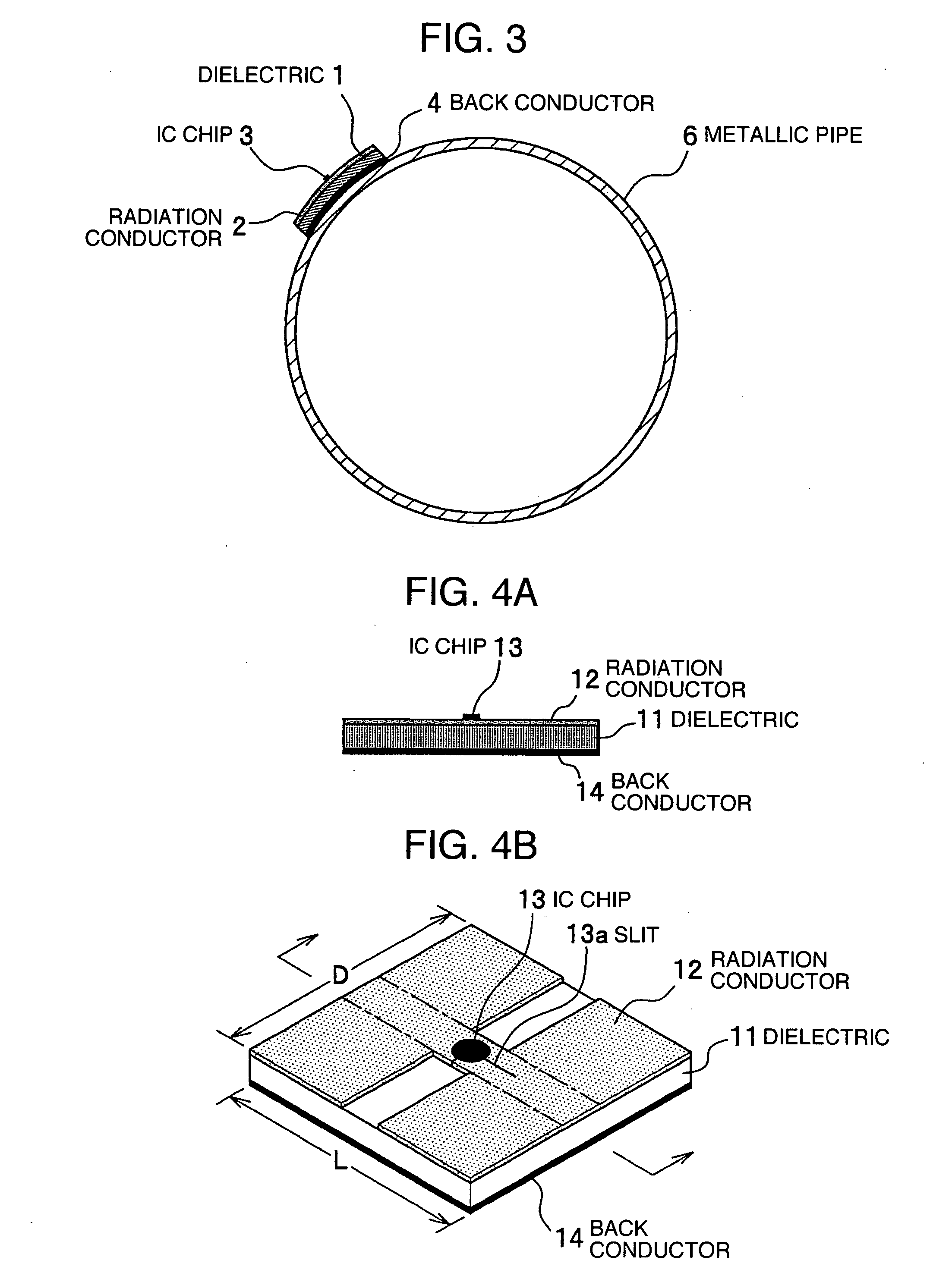
[0045]FIGS. 4A and 4B show a micro-strip antenna of a radio wave IC tag according to the second embodiment of the invention. FIG. 4A is a sectional view and FIG. 4B is a perspective view. An H-shaped radiation conductor 12 is formed on the entire surface of a dielectric 11 and a back conductor 14 is formed on the entire back surface of the dielectric 11. An IC chip 13 is mounted to a contraction (narrowed) portion of the H-shaped radiation conductor 12 on the front surface side. Incidentally, an L-shaped slit 13a is formed at the contraction portion of the radiation conductor 12 to which the IC chip 13 is mounted. The slit 13a is for preventing dielectric breakdown and for establishing impedance matching in the same way as in the first embodiment.

[0046] The H-shaped radiation conductor 12 formed on the front surface of the dielectric 11 operates as a micro-strip antenna in cooperation with the back conductor 14 that is formed on the entire back surface of the dielectric 11. Since t...

third embodiment

[0049] A round IC tag will be explained in the third embodiment. To have the explanation more easily understood, the round radio wave IC tag of the third embodiment will be explained in comparison with a radio wave IC tag of the Comparative Example. FIGS. 5A to 5D are structural views of round radio frequency IC tags according to Comparative Example and to the third embodiment of the invention, wherein FIG. 5A is a sectional view of the radio frequency IC tag of Comparative Example, FIG. 5B is a perspective view of the radio frequency IC tag of Comparative Example, FIG. 5C is a sectional view of the radio frequency IC tag of the third embodiment and FIG. 5D is a perspective view of the radio frequency IC tag of the third embodiment, respectively.

[0050] To let the radio frequency IC tag of Comparative Example operate as the micro-strip antenna, a round H-shaped radiation conductor 132a is formed at the center of a disk-like dielectric 131a having a large area as shown in FIGS. 5A an...


PUM


Abstract

A radio frequency IC tag has wide directivity and is rich in flexibility. A radiation conductor is formed on the entire surface of a dielectric formed of synthetic resin foam and a back conductor is formed on the entire back surface of the dielectric. An IC chip is mounted to the radiation conductor on the front side. An L-shaped slit is formed at the portion of the radiation conductor at which the IC chip is mounted. The radiation conductor and the back conductor have the same size or the size of the back conductor is not greater than twice the size of the radiation conductor.

Description

CROSS-REFERENCE TO RELATED APPLICATION [0001] The present invention contains subject matter which is related to the subject matter of U.S. patent application Ser. No. (not yet assigned) filed Dec. —, 2005 claiming the priority from Japanese patent application No. 2005-158110 filed on May 30, 2005 and entitled “RADIO FREQUENCY IC TAG AND METHOD FOR MANUFACTURING SAME”, by Isao Sakama and Minoru Ashizawa and assigned to the same assignee of the present application, the disclosure of which is hereby incorporated by reference herein. INCORPORATION BY REFERENCE [0002] The present application claims priority from Japanese application JP 2005-133438 filed on Apr. 28, 2005, the content of which is hereby incorporated by reference into this application. BACKGROUND OF THE INVENTION [0003] This invention relates to a radio frequency IC tag for wireless transmission of information recorded to an IC chip. More particularly, the invention relates to a radio frequency IC tag using an improved ante...

Claims


Application Information

Patent Timeline
Patent Type & Authority Applications(United States)
IPC IPC(8): G08B13/14
CPCH01Q1/22H01Q23/00H01Q9/04H01Q1/38F16B23/0015F16B35/06
Inventor SAKAMA, ISAOASHIZAWA, MINORU
Owner HITACHI LTD
Why Eureka
Try Eureka