
Field effect transistor device including an array of channel elements and methods for forming

a field effect transistor and array technology, applied in the field of semiconductor devices, can solve the problems of inability to achieve the same packing density limitations as previously described, and achieve the effect of optimal device structure and better control of element dimensions

Inactive Publication Date: 2006-11-09
GLOBALFOUNDRIES INC
View PDF5 Cites 138 Cited by
  • Summary
  • Abstract
  • Description
  • Claims
  • Application Information

AI Technical Summary

Benefits of technology

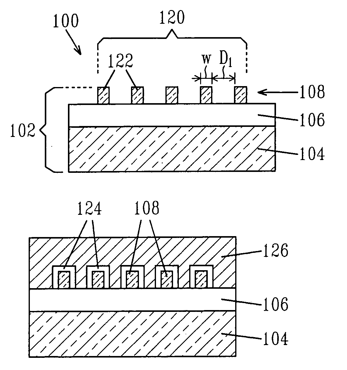
[0021] Achieving improvements over the conventional means of forming the channel array FETs described above requires better control over element dimensions and efficient packing of device channel elements into arrays in which the spacing between each element is uniform and regular. The present invention provides a method for achieving these improvements, which leads to the optimal device structure.

Problems solved by technology

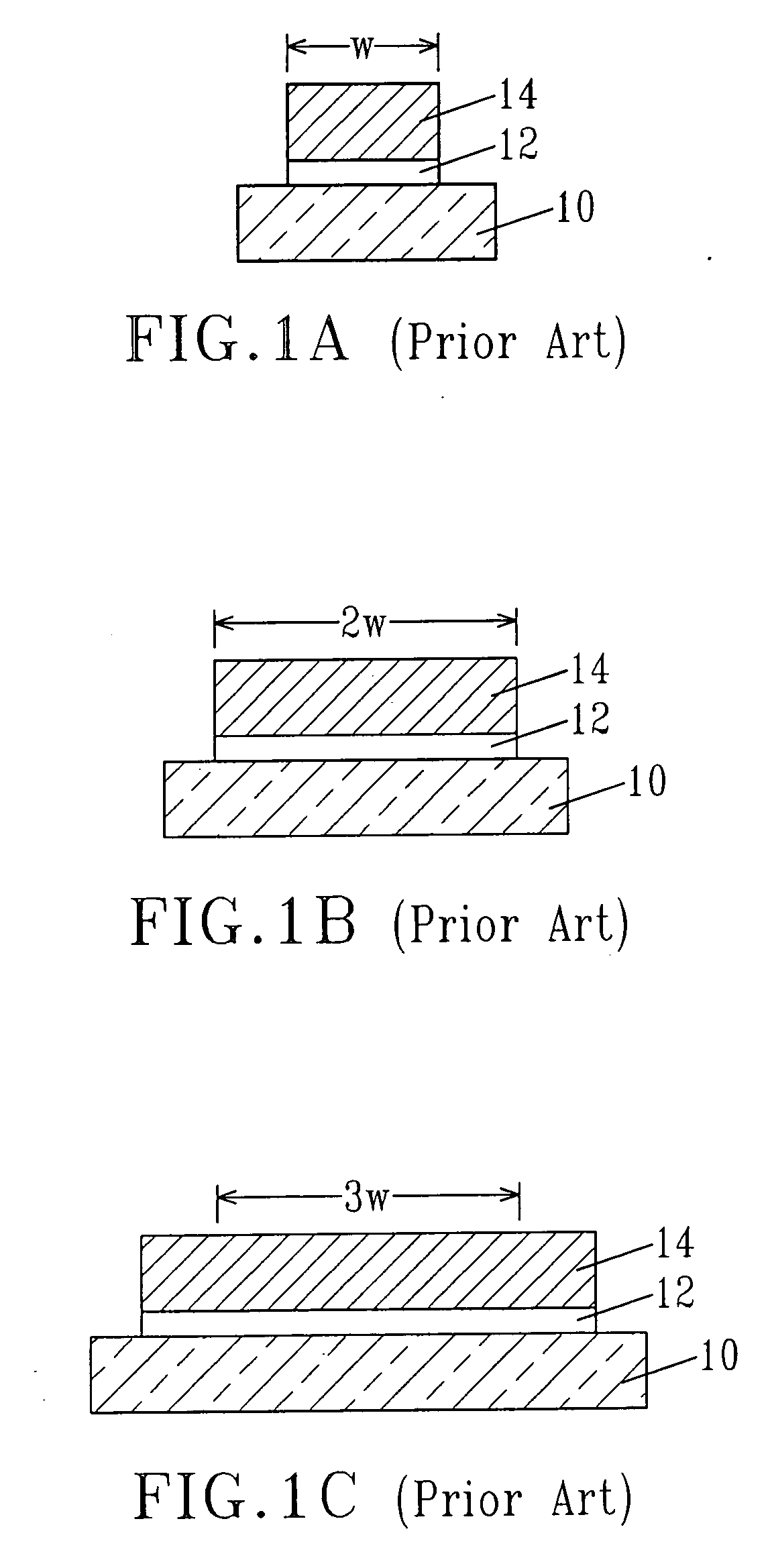
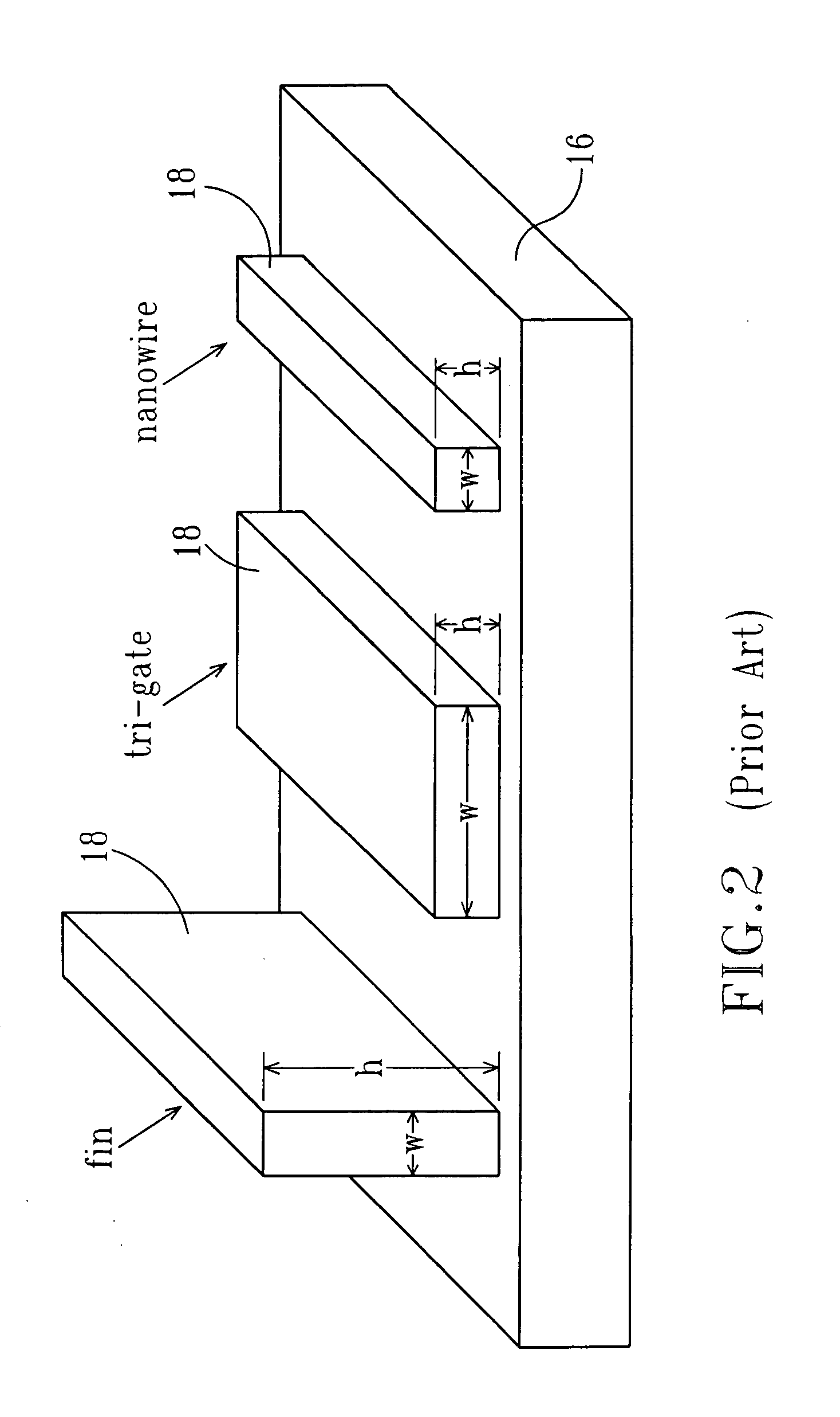
As mentioned above, previous demonstrations have used oxygen plasma trimming or sidewall spacer processes to define the widths of FET channel elements—these techniques have the inherent limitations on packing density as previously described.

Method used


Image

  • Field effect transistor device including an array of channel elements and methods for forming
  • Field effect transistor device including an array of channel elements and methods for forming
  • Field effect transistor device including an array of channel elements and methods for forming

Examples


embodiment 1

[0079] Method 1 (Embodiment 1): This method utilizes an asymmetric A-B diblock copolymer in which block A is present as the majority component and block B is present in lesser amounts than block A. In these examples, the polymer block B is one which can be preferentially removed from the film, e.g., by exposure to UV radiation and immersion in a chemical solvent, or by exposure to ozone. When a polymer of this composition is applied to a surface containing a lithographically defined topography (FIG. 9A), a resulting line / space pattern forms in which half-cylinders of block B are embedded in a matrix of block A. The resulting pattern self aligns with the preexisting topography. Removal of block B leaves the lithographically-defined line subdivided into periods of the underlying block A matrix. This is illustrated in FIG. 9B.

embodiment 2

[0080] Method 2 (Embodiment 2): This method utilizes an asymmetric A-B diblock copolymer in which block A is present as the minority component and block B is present in a greater amount. In these examples, the polymer block B is one which can be preferentially removed from the film, e.g., by exposure to UV radiation and immersion in a chemical solvent, or by exposure to ozone. When a polymer of this composition is applied to a surface containing a lithographically defined topography (FIG. 10A), a resulting line / space pattern forms in which half-cylinders of block A are embedded in a matrix of block B. The resulting pattern self aligns with the preexisting topography. Removal of block B leaves the lithographically-defined line subdivided into periods of the underlying block A matrix. This is illustrated in FIG. 10B.

embodiment 3

[0081] Method 3 (Embodiment 3): Symmetric A-B diblock copolymer is used and is applied within an opening as discussed above. In this example, blocks A and B have substantially the same weight % in the total block copolymer and block B is a block which can be preferentially removed from the polymer film, e.g., by exposure to UV radiation and immersion in a chemical solvent, or by exposure to ozone. When a polymer of this composition is applied to a surface containing a lithographically defined topography (FIG. 11A), a resulting line / space pattern forms in which lines / spaces of block A are embedded in a matrix of block B. The resulting pattern self aligns with the preexisting topography. Removal of block B leaves the lithographically-defined line subdivided into periods of the underlying block A matrix. This is illustrated in FIG. 11 B.

[0082] After the array pattern is formed in the diblock copolymer material using any of the three above-described methods, it can be used to template t...


PUM


Abstract

The present invention relates to a semiconductor structure such as a field effect transistors (FETs) in which the channel region of each of the FETs is composed of an array of more than one electrically isolated channel. In accordance with the present invention, the distance between each of the channels present in the channel region is within a distance of no more than twice their width from each other. The FETs of the present invention are fabricated using methods in which self-assembled block copolymers are employed in forming the channel.

Description

FIELD OF THE INVENTION [0001] The present invention relates to semiconductor devices and methods of fabricating the same. More particularly, the present invention relates to field effect transistors (FETs) in which the channel region of each of the FETs is composed of an array of more than one electrically isolated channel. In accordance with the present invention, the distance between each neighboring channel is less than or equal to twice the width of an individual channel within the array. The FETs of the present invention are fabricated using methods in which self-assembled block copolymers are employed in forming the channel region. BACKGROUND OF THE INVENTION [0002] The dimensions of semiconductor field effect transistors (FETs) have been steadily shrinking over the last thirty 30 years or so, as scaling to smaller dimensions leads to continuing device performance improvements. Planar FET devices have a conducting gate electrode positioned above a semiconducting channel, and e...

Claims


Application Information

Patent Timeline
IPC IPC(8): H01L29/76
CPCH01L29/0673H01L29/66795H01L29/78684H01L29/78681H01L29/785Y10S438/949Y10S438/947Y10S438/948Y10S438/945
Inventor BLACK, CHARLES T.RUIZ, RICARDO
Owner GLOBALFOUNDRIES INC
Learn More