Semiconductor device and manufacturing method of the same

a semiconductor device and manufacturing method technology, applied in the field of semiconductor devices, can solve problems such as reducing the yield of semiconductor devices, and achieve the effect of increasing the yield

Active Publication Date: 2006-11-09
SEMICON COMPONENTS IND LLC
View PDF12 Cites 24 Cited by
  • Summary
  • Abstract
  • Description
  • Claims
  • Application Information

AI Technical Summary

Benefits of technology

[0017] The invention provides a semiconductor device with a bonding pad made of a wiring layer including aluminum and its manufacturing method that enhance the yield of the semiconductor device.
[0027] The invention can prevent metal that forms the wiring layer from being eluted to form a defect portion or deposit an eluted component. Therefore, when a wire is bonded to the wiring layer, a connection failure as has been seen in the conventional art can be prevented. As a result, the yield can be increased by this semiconductor device with the bonding pad made of a wiring layer including aluminum and its manufacturing method.

Problems solved by technology

As a result, a connection failure occurs between the second wiring layer 22 as the bonding pad and the lead frame (not shown) when a wire is bonded thereto, reducing the yield of the semiconductor device.

Method used


Image

  • Semiconductor device and manufacturing method of the same
  • Semiconductor device and manufacturing method of the same
  • Semiconductor device and manufacturing method of the same

Examples


first embodiment

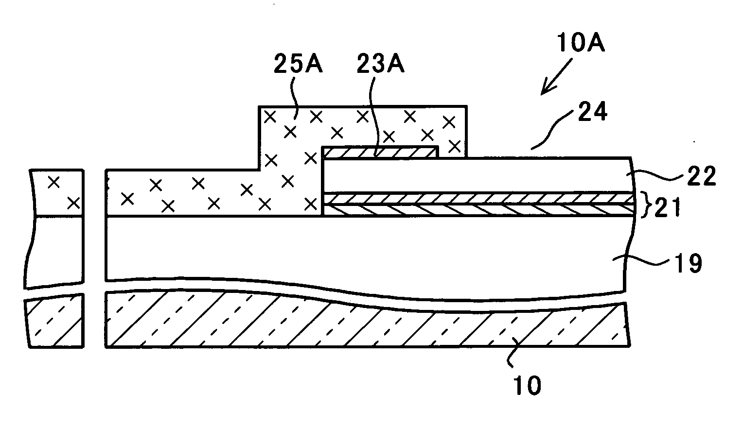
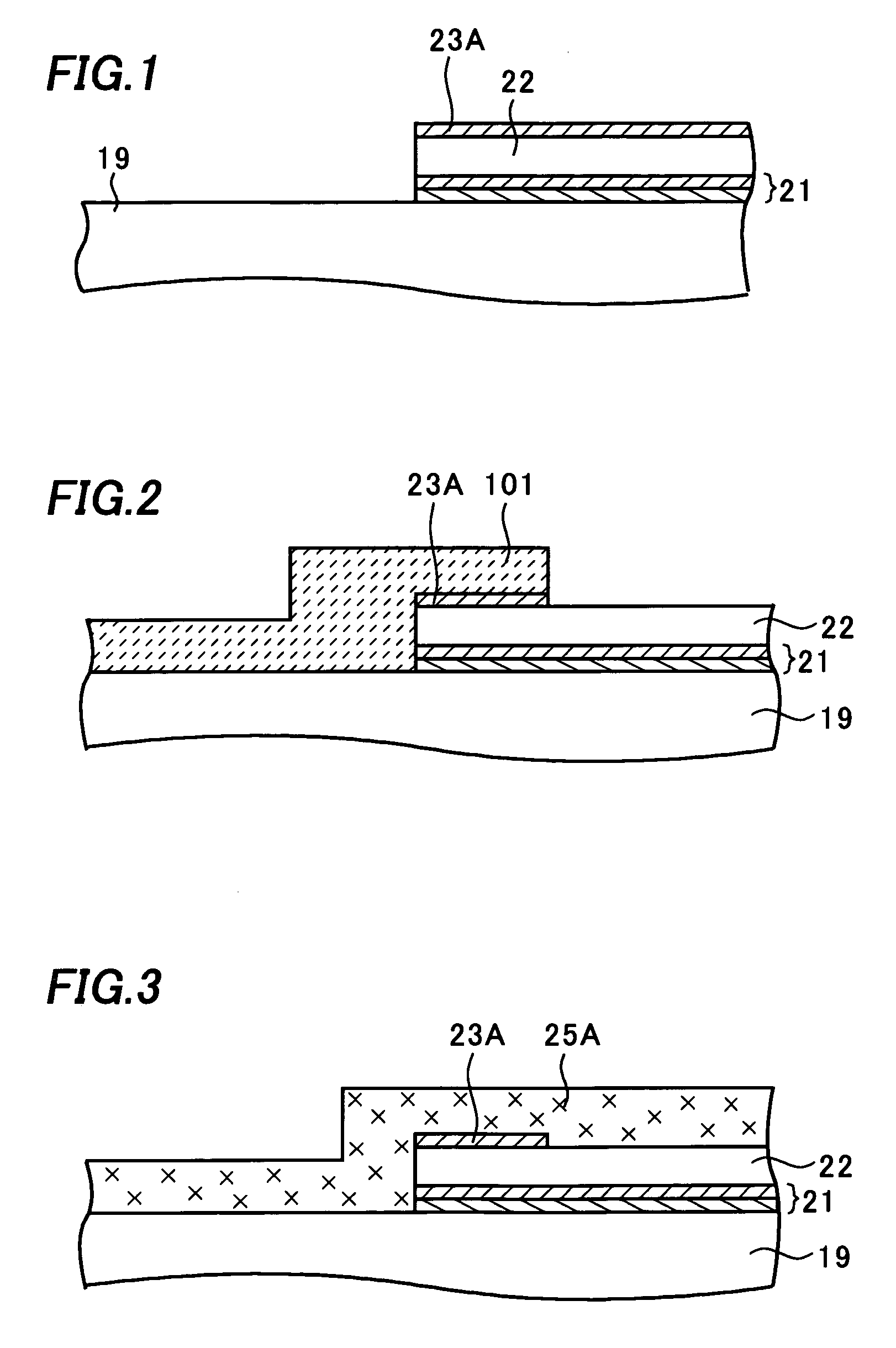
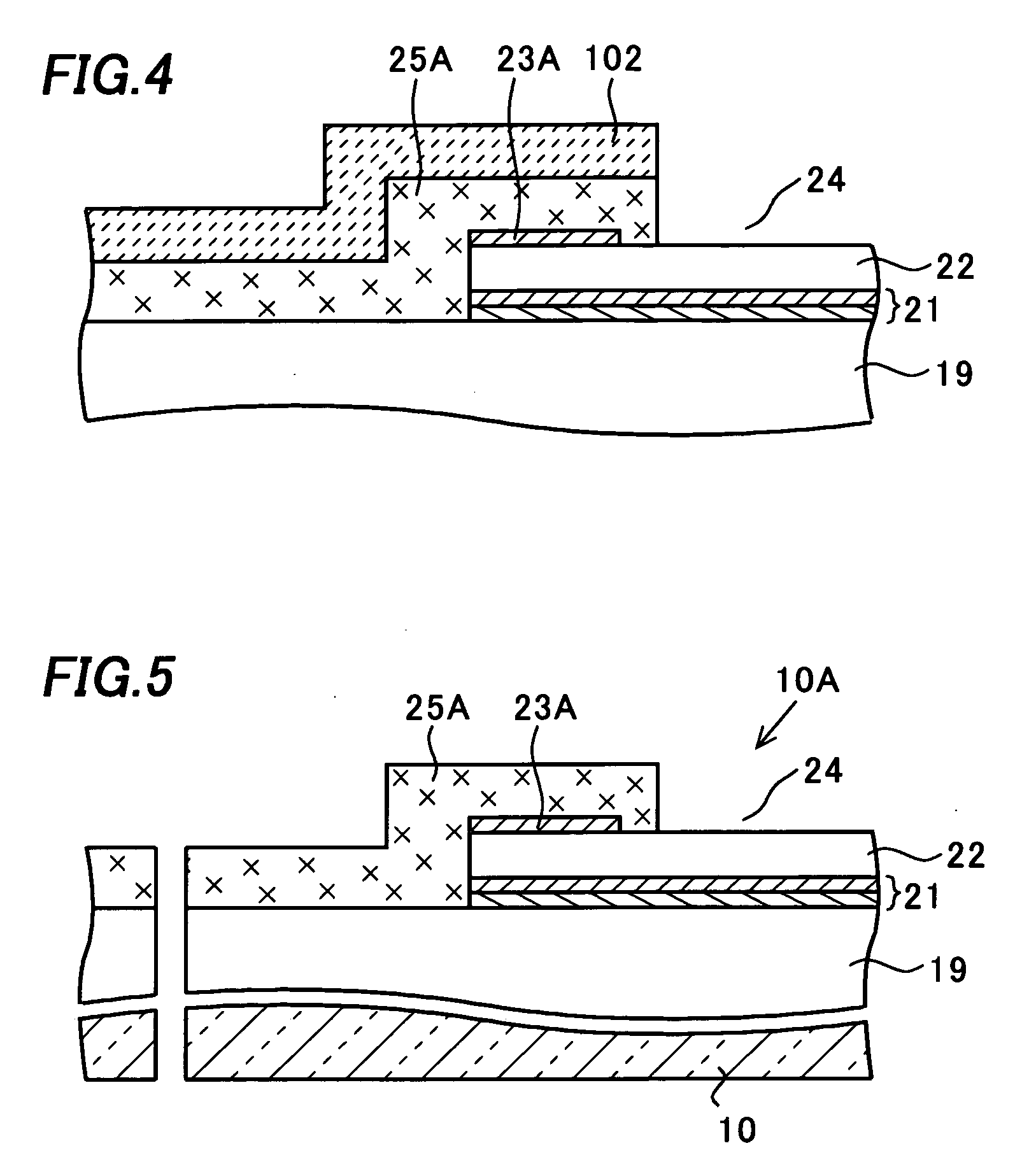
[0044] A semiconductor device of the invention will be described referring to figures. FIGS. 1 to 4 are cross-sectional views showing a method of manufacturing the semiconductor device of this embodiment. FIG. 5 is a cross-sectional view showing the semiconductor device and its manufacturing method of this embodiment.

[0045] The semiconductor device of this embodiment has the same components as the conventional semiconductor device shown in FIG. 40 from the semiconductor substrate 10 to the second wiring layer 22. Therefore, the description of the semiconductor device of this embodiment will be made on the components formed above the second wiring layer 22 only in FIGS. 1 to 5. The components formed below the second interlayer insulation film 19 are omitted in the figures.

[0046] A second wiring layer 22 and an antireflection layer 23A are formed into a predetermined pattern through patterning processes including a photolithography (exposure and development of a resist layer (not sho...

second embodiment

[0055] Next, a semiconductor device of the invention will be described referring to figures. FIGS. 6 to 9 are cross-sectional views showing a method of manufacturing the semiconductor device of this embodiment. FIG. 10 is a cross-sectional view showing the semiconductor device and its manufacturing method of this embodiment.

[0056] The description of the semiconductor device of this embodiment will be made on the components formed above the second wiring layer 22 only in FIGS. 6 to 10, as in the first embodiment. The other components and the manufacturing method thereof are the same as those of the conventional art shown in FIG. 40. The components formed below the second interlayer insulation film 19 are omitted in the figures.

[0057] The second wiring layer 22 and an antireflection layer 23B are formed into a predetermined pattern through patterning processes including a photolithography, as shown in FIG. 6. The antireflection layer 23B is made of the same metal as the antireflectio...

third embodiment

[0063] Next, a semiconductor device of the invention will be described referring to figures. FIGS. 11 to 15 are cross-sectional views showing a method of manufacturing the semiconductor device of this embodiment. FIG. 16 is a cross-sectional view showing the semiconductor device and its manufacturing method of this embodiment.

[0064] The description of the semiconductor device of this embodiment will be made on the components formed above the second wiring layer 22 only in FIGS. 11 to 16, as in the first embodiment. The other components and the manufacturing method thereof are the same as those of the conventional art shown in FIG. 40. The components formed below the second interlayer insulation film 19 are omitted in the figures.

[0065] The second wiring layer 22 and an antireflection layer 23C are formed into a predetermined pattern through patterning processes including a photolithography, as shown in FIG. 11. The antireflection layer 23C is made of the same metal as the antirefle...


PUM


Abstract

The invention provides a semiconductor device with a bonding pad made of a wiring layer including aluminum and its manufacturing method that enhance the yield of the semiconductor device. The method of manufacturing the semiconductor device of the invention includes removing a portion of an antireflection layer (e.g. made of a titanium alloy) formed on an uppermost second wiring layer (e.g. made of aluminum) on a semiconductor substrate by etching, forming a passivation layer covering the antireflection layer and a portion of the second wiring layer where the antireflection layer is not formed and having an opening exposing the other portion of the second wiring layer, and dividing the semiconductor substrate into a plurality of semiconductor dice by dicing. These processes can prevent the antireflection layer from being exposed in the opening, and this can prevent a component of the second wiring layer from being eluted due to cell reaction between the second wiring layer and the antireflection layer as has been seen in the conventional art.

Description

CROSS-REFERENCE OF THE INVENTION [0001] This invention is based on Japanese Patent Application No. 2005-087685 and No. 2006-045448, the content of which is incorporated herein by reference in its entirety. BACKGROUND OF THE INVENTION [0002] 1. Field of the Invention [0003] The invention relates to a semiconductor device and its manufacturing method, particularly, a semiconductor device with a bonding pad made of a wiring layer including aluminum and its manufacturing method. [0004] 2. Description of the Related Art [0005] A bonding pad has been known as an electrode for external connection of an input / output terminal or a power supply terminal of a semiconductor integrated circuit or the like. The bonding pad is formed using an aluminum (Al) wiring, for example, and connected with a lead frame or the like through a bonding wire or the like. [0006] Next, a conventional semiconductor device with the bonding pad made of an aluminum (Al) wiring will be described referring to figures. FI...

Claims


Application Information

Patent Timeline
Patent Type & Authority Applications(United States)
IPC IPC(8): H01L23/48H01L21/44
CPCH01L23/3192H01L24/03H01L2224/48747H01L2224/48724H01L2924/01006H01L2924/19043H01L2924/14H01L2924/05042H01L2924/04941H01L2924/01082H01L2924/0105H01L2924/01033H01L2924/01029H01L2924/01027H01L2924/01022H01L2924/01018H01L2924/01014H01L2924/01013H01L2924/01005H01L2924/01004H01L2224/48463H01L24/05H01L24/48H01L2224/04042H01L2224/05082H01L2224/05138H01L2224/05166H01L2224/05187H01L2224/05624H01L2224/05647H01L2224/45124H01L2924/00014H01L2924/04953H01L2924/00H01L2224/02166H01L2224/45099H01L2924/00015F16L3/13F16L3/1211
Inventor TAKAI, NOBUYUKISUZUKI, TAKUYATSUKADA, YUJI
Owner SEMICON COMPONENTS IND LLC
Why Eureka
Try Eureka