Unlock instant, AI-driven research and patent intelligence for your innovation.

Output impedance circuit and output buffer circuit including the same

a buffer circuit and output impedance technology, applied in logic circuits, pulse techniques, reliability increasing modifications, etc., can solve problems such as error caused by reflected signals, impedance differences, and error caused by errors

Active Publication Date: 2006-11-09
SAMSUNG ELECTRONICS CO LTD
View PDF7 Cites 0 Cited by
  • Summary
  • Abstract
  • Description
  • Claims
  • Application Information

AI Technical Summary

Benefits of technology

The present invention provides an output impedance circuit and an output buffer circuit that can function stably regardless of changes in manufacturing process and can have a desired output impedance regardless of a pad voltage. The output impedance circuit includes an output stage and an impedance control stage. The output stage supplies a current to the output terminal based on a DC bias voltage, while the impedance control stage controls the current flowing through the output stage in response to the output signal. The output buffer circuit includes an impedance circuit with a regular impedance component at the output terminal and a driving transistor. The output impedance circuit also includes an on / off selecting device and an inverse control signal for selecting the operation state of the output impedance circuit. The technical effects of the present invention are stable operation and desired output impedance regardless of changes in manufacturing process and pad voltage.

Problems solved by technology

However, error may be caused by an impedance differences when using conventional output impedance circuit 100.
The error may include, error caused by reflected signals that are not transmitted.
Further, because second and third P-type MOS transistors P2 and P3 may operate in a saturation region, an amount of current may drastically increase according to the pad PAD voltage, and thus an impedance component may be excessively reduced in a low pad PAD voltage.

Method used


Image

  • Output impedance circuit and output buffer circuit including the same
  • Output impedance circuit and output buffer circuit including the same
  • Output impedance circuit and output buffer circuit including the same

Examples


Embodiment Construction

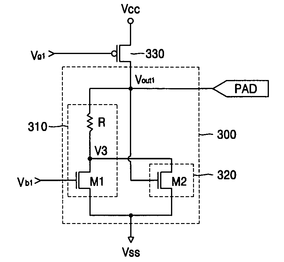
[0033] Various example embodiments of the present invention will now be described more fully with reference to the accompanying drawings in which some example embodiments of the invention are shown.

[0034] Detailed illustrative embodiments of the present invention are disclosed herein. However, specific structural and functional details disclosed herein are merely representative for purposes of describing example embodiments of the present invention. This invention may, however, may be embodied in many alternate forms and should not be construed as limited to only the embodiments set forth herein.

[0035] Accordingly, while example embodiments of the invention are capable of various modifications and alternative forms, embodiments thereof are shown by way of example in the drawings and will herein be described in detail. It should be understood, however, that there is no intent to limit example embodiments of the invention to the particular forms disclosed, but on the contrary, examp...


PUM


Abstract

Provided is an output impedance circuit, which has a constant output impedance regardless of a pad voltage, and an output buffer circuit including the output impedance circuit. The output impedance circuit includes an output stage and an impedance control stage. The output stage outputs a current corresponding to a DC bias voltage via an output terminal, and the impedance control stage controls the current flowing through the output stage in response to an output signal. The output stage includes a resistance component and a first MOS transistor. A first terminal of the resistance component is connected to the output terminal. A first terminal of the first MOS transistor is connected to a second terminal of the resistance component, a second terminal of the first MOS transistor is connected to a voltage source, and an input signal is input to a gate of the first MOS transistor.

Description

PRIORITY STATEMENT [0001] This application claims the priority of Korean Patent Application No. 10-2005-0009103, filed on Feb. 1, 2005 in the Korean Intellectual Property Office, the entire contents of which are incorporated herein by reference. FIELD OF THE INVENTION [0002] The present invention relates to an output impedance circuit of a semiconductor device, and more particularly, to an output impedance circuit having an output impedance load with linear characteristics regardless of which system is connected to the output impedance circuit, and an output buffer circuit including the same. DESCRIPTION OF THE RELATED ART [0003]FIG. 1 is a diagram of a conventional output impedance circuit 100. As shown in FIG. 1, a conventional output impedance circuit 100 may include three P-type MOS transistors, first, second, and third P-type MOS transistors P1 through P3, and a resistor R. A fourth MOS transistor P4 may invert an input voltage Vg applied to its gate, the MOS transistor P4 may ...

Claims


Application Information

Patent Timeline
Patent Type & Authority Applications(United States)
IPC IPC(8): H03K19/003
CPCH03K19/0005H03K19/0175
Inventor KIM, TAE-HYOUNGCHO, UK-RAE
Owner SAMSUNG ELECTRONICS CO LTD