
Display device

a display device and resistor technology, applied in the direction of static indicating devices, instruments, etc., can solve the problems of degrading the display image quality of the display image displayed on the liquid crystal display panel, fluctuating the gray scale voltage, etc., to prevent the degradation of the image quality of the display image, reduce the voltage dependency of the semiconductor resistance element, and reduce power consumption

Inactive Publication Date: 2006-11-09
HITACHI DISPLAYS
View PDF3 Cites 1 Cited by
  • Summary
  • Abstract
  • Description
  • Claims
  • Application Information

AI Technical Summary

Benefits of technology

[0017] To briefly explain advantageous effects obtained by the typical inventions among the inventions disclosed in this specification, they are as follows.
[0018] According to the display device of the present invention, it is possible to reduce the voltage dependency of the semiconductor resistance element.
[0019] Accordingly, by using the semiconductor resistance element in a resistance voltage dividing circuit, it is possible to prevent the degradation of image quality of a display image displayed on the display element and to realize the reduction of power consumption.

Problems solved by technology

Accordingly, when the semiconductor resistance element is used as the voltage dividing resistance of a resistance voltage dividing circuit for generating gray scale voltages in a driver of a liquid crystal display device, there has been a drawback that the gray scale voltages are fluctuated thus degrading display quality of a display image which is displayed on a liquid crystal display panel.

Method used


Image

  • Display device
  • Display device
  • Display device

Examples


Embodiment Construction

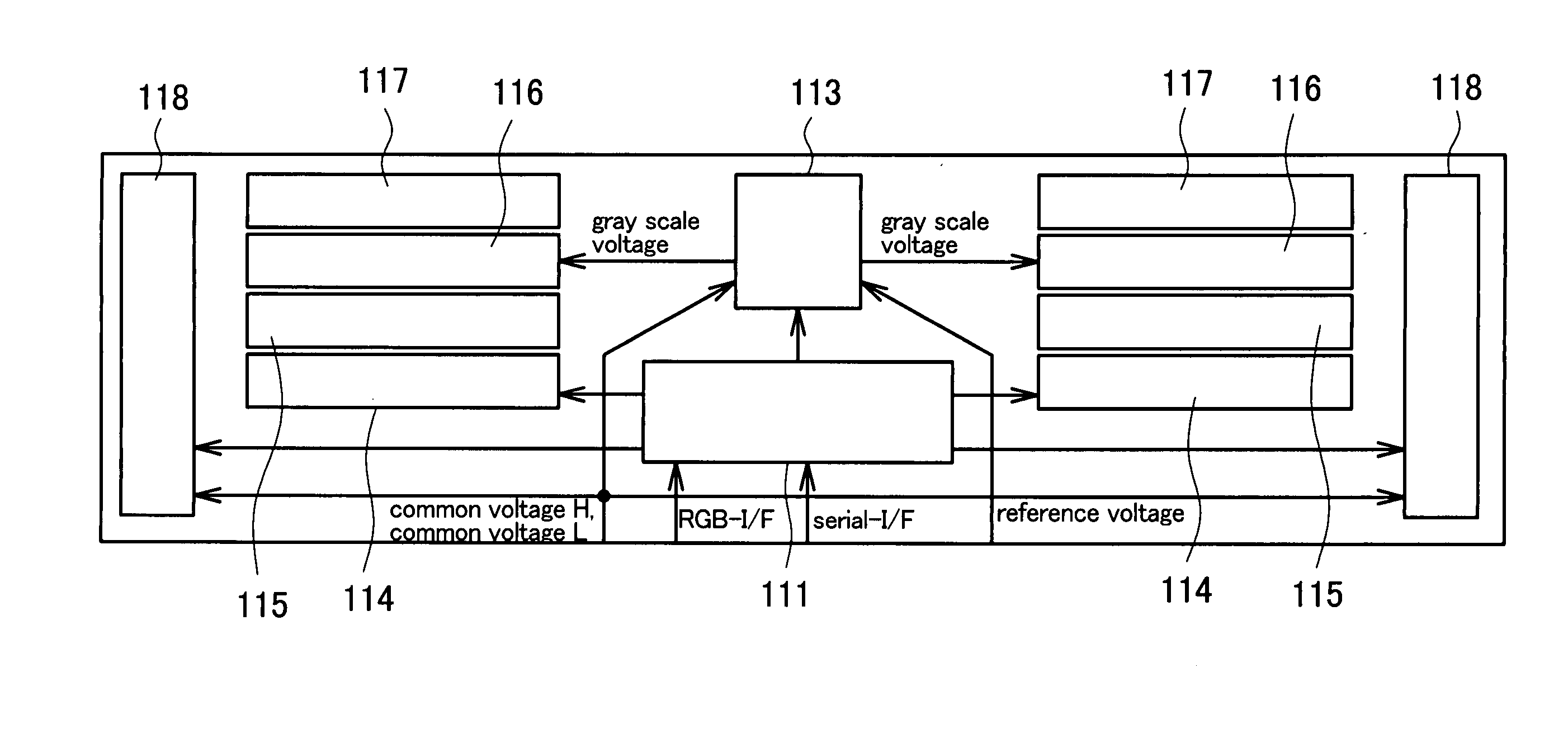
[0032] Embodiments in which the present invention is applied to a liquid crystal display module are explained in detail in conjunction with drawings hereinafter.

[0033] Here, in all drawings for explaining the embodiments, parts having identical functions are given same symbols and their repeated explanation is omitted.

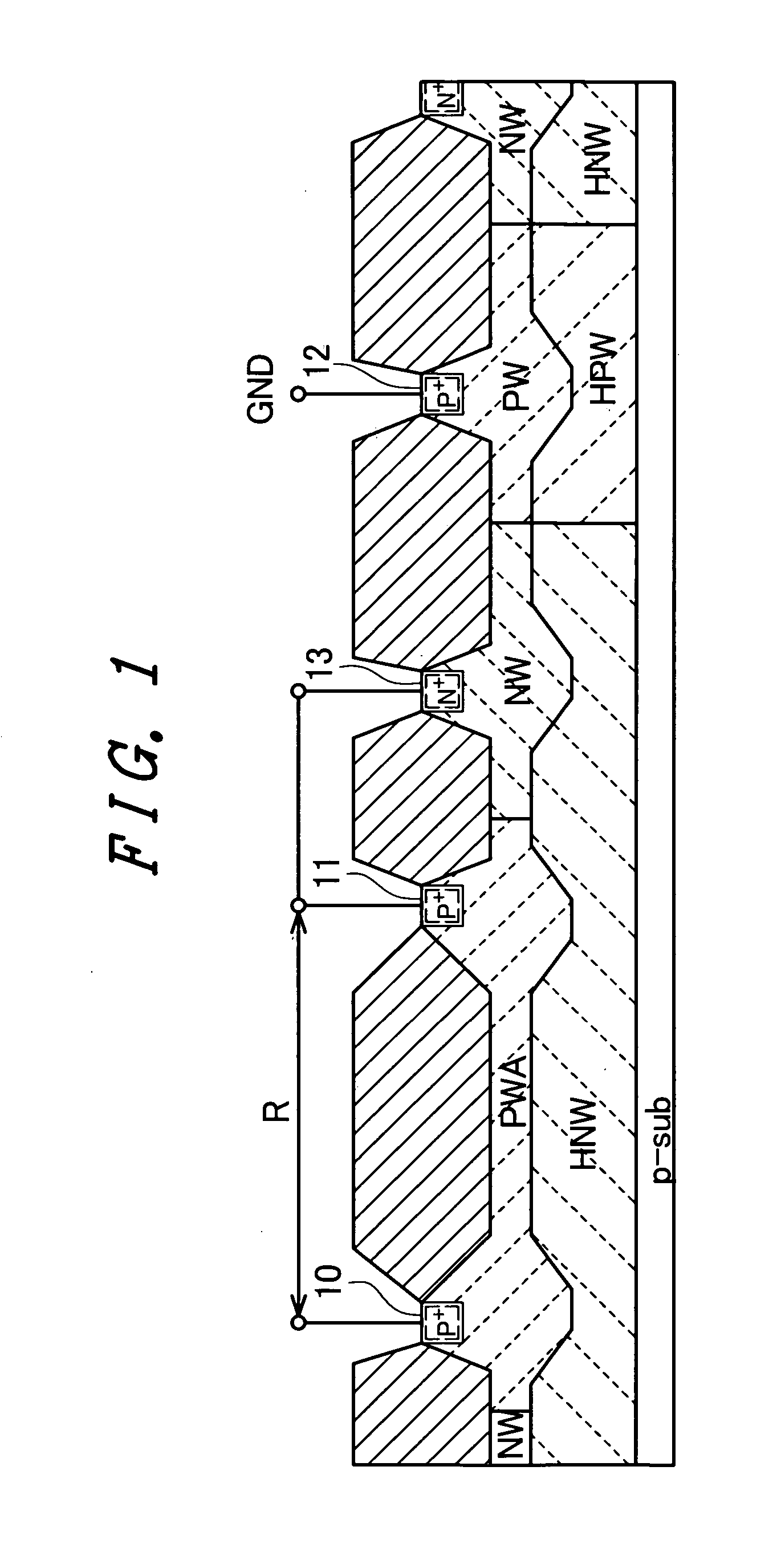
[0034]FIG. 1 is a cross-sectional view of an essential part showing one example of a semiconductor resistance element used in a liquid crystal display module of an embodiment of the present invention.

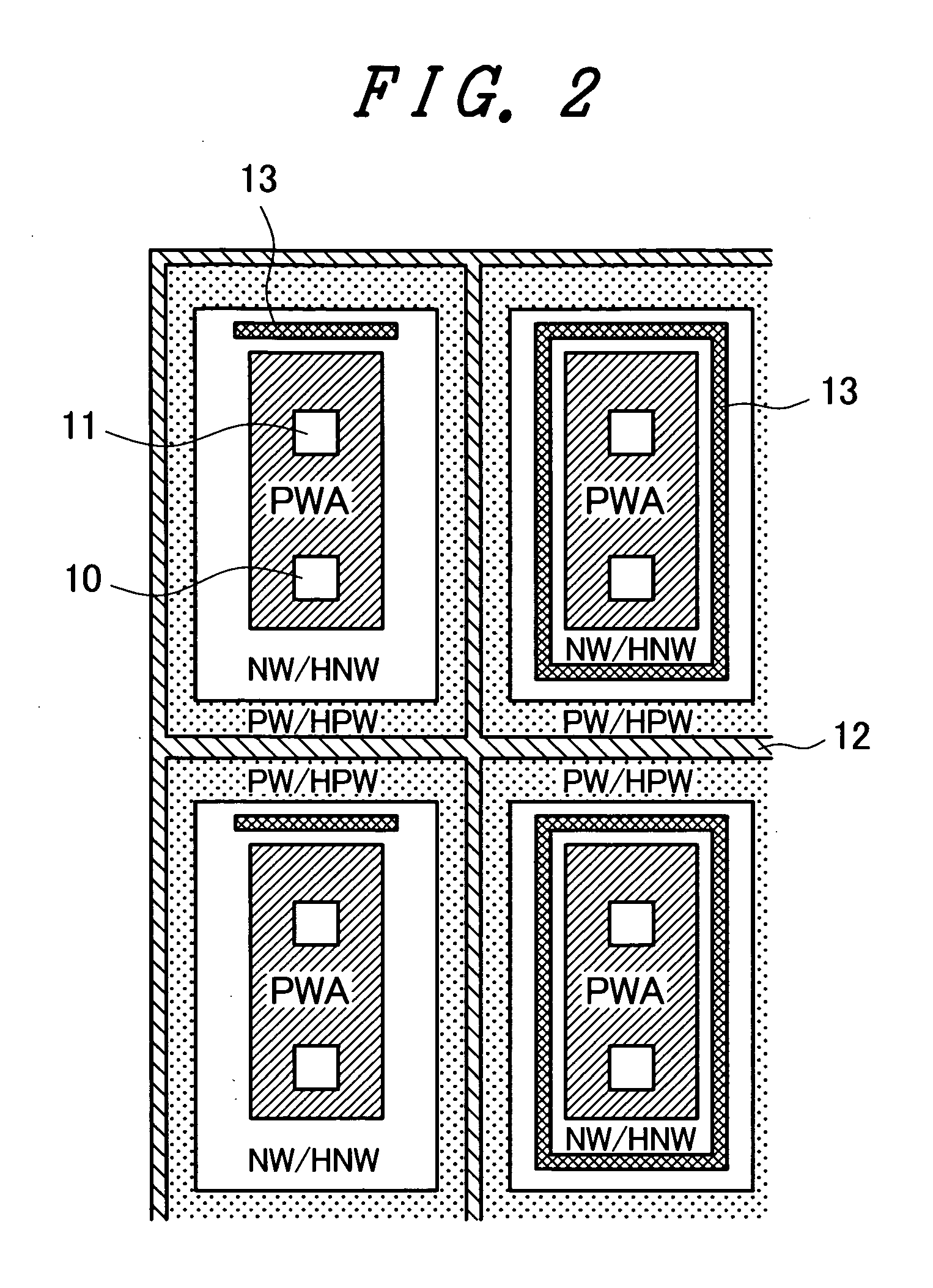
[0035] In the drawing, symbol p-sub indicates a p-type semiconductor substrate, symbol PWA indicates a p-type well region (ap-type impurity region) which functions as a resistance element, symbol NW indicates an n-type well region (an n-type impurity region), symbol HNW indicates an n-type well region which is formed deeper than the n-type well region (NW), symbol PW indicates a p-type well region which constitutes a separation layer, symbol HPW indicates a p-type well ...


PUM


Abstract

The present invention decreases the voltage dependency of a semiconductor resistance element used in a resistance voltage dividing circuit thus preventing the deterioration of display quality of a display image and, at the same time, realizing the reduction of power consumption. In a display device which includes a display element and a drive circuit which drives the display element, the drive circuit includes a semiconductor resistance element, the semiconductor resistance element includes a first conductive impurity region and a second conductive impurity region which is embedded in the first conductive impurity region and functions as a resistance element, the second conductive impurity region includes a first electrode and a second electrode, and a voltage which is applied to the first electrode or the second electrode of the second conductive impurity region is applied to the first conductive impurity region.

Description

BACKGROUND OF THE INVENTION [0001] 1. Field of the Invention [0002] The present invention relates to a display device, and more particularly to a resistance dividing circuit for generating gray scale reference voltages. [0003] 2. Description of Related Art [0004] In a liquid crystal display device, gray scale voltages corresponding to display data are selected by a decoder circuit in the inside of a driver, and the gray scale voltages are supplied to a liquid crystal panel so as to allow the liquid crystal panel to display an image. The gray scale voltages are, for example, generated by a resistance voltage dividing circuit which uses ladder resistances in the inside of the driver. [0005] However, when the ladder resistances are used, a direct-current (DC) current is generated and hence, with respect to a digital camera or a portable-use liquid crystal display device which is required to satisfy a strong demand for low power consumption, it is necessary to increase the ladder resist...

Claims


Application Information

Patent Timeline
IPC IPC(8): G09G3/36
CPCG09G3/2011G09G2330/021G09G2300/0408G09G3/3685
Inventor KOTANI, YOSHIHIROKIDA, HIDETOSHIAGATA, KENTARONAKAYASU, YOUZOUWATANABE, HIROSHI
Owner HITACHI DISPLAYS
Learn More