Memory-based Fast Fourier Transform device

a fourier transform and memory-based technology, applied in the field of single-port ram-based fft devices, can solve the problems of high computational complexity, computational complexity, and the circuit area of the fft device b>10/b> is still large and needs to be further reduced, so as to reduce the required circuit area

Inactive Publication Date: 2006-11-09
IND TECH RES INST
View PDF14 Cites 18 Cited by
  • Summary
  • Abstract
  • Description
  • Claims
  • Application Information

AI Technical Summary

Benefits of technology

[0016] The object of the invention is to provide a memory-based FFT de

Problems solved by technology

However, equation (1) obviously implies the problem of high computational complexity to thus be replaced by FFT, which has a merit of lower computational complexity.

Method used


Image

  • Memory-based Fast Fourier Transform device
  • Memory-based Fast Fourier Transform device
  • Memory-based Fast Fourier Transform device

Examples


Embodiment Construction

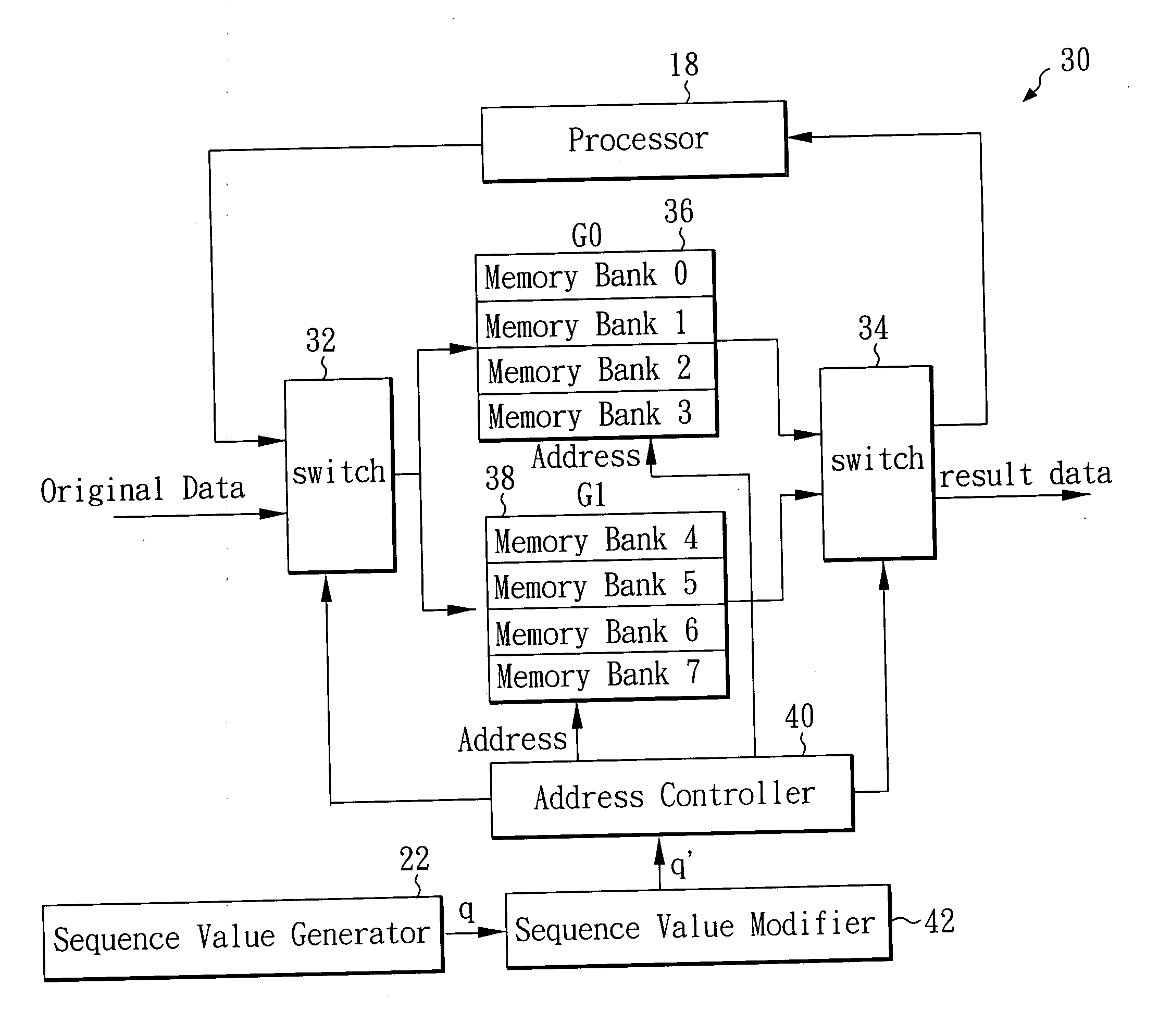
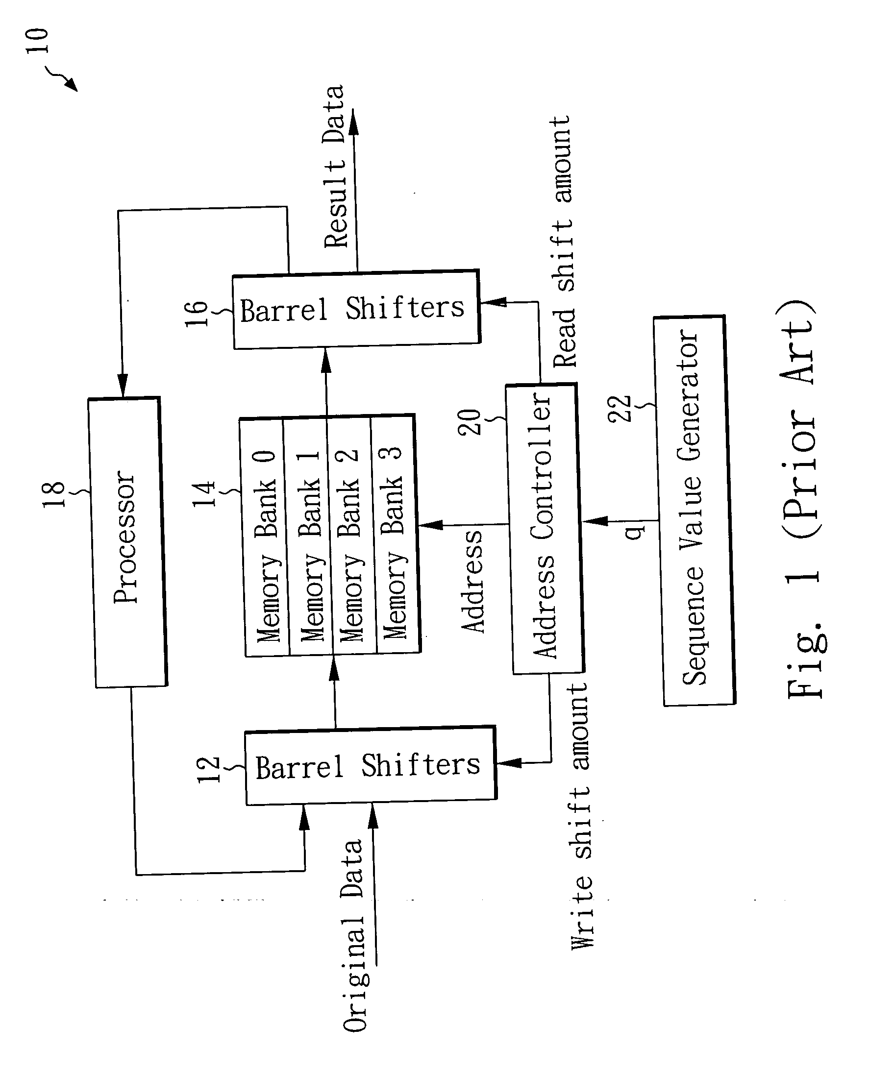
[0030] Since a traditional memory 14 of an N-point FFT device 10 is implemented by dual port RAM banks, and a cell of each dual port RAM bank typically contains 16 transistors, in order to achieve the purpose of reducing the circuit area of the device 10, the invention replaces the dual port RAM banks with single port RAM banks, a cell of each single port RAM bank containing just about ten transistors. Thus, the circuit area is significantly reduced.

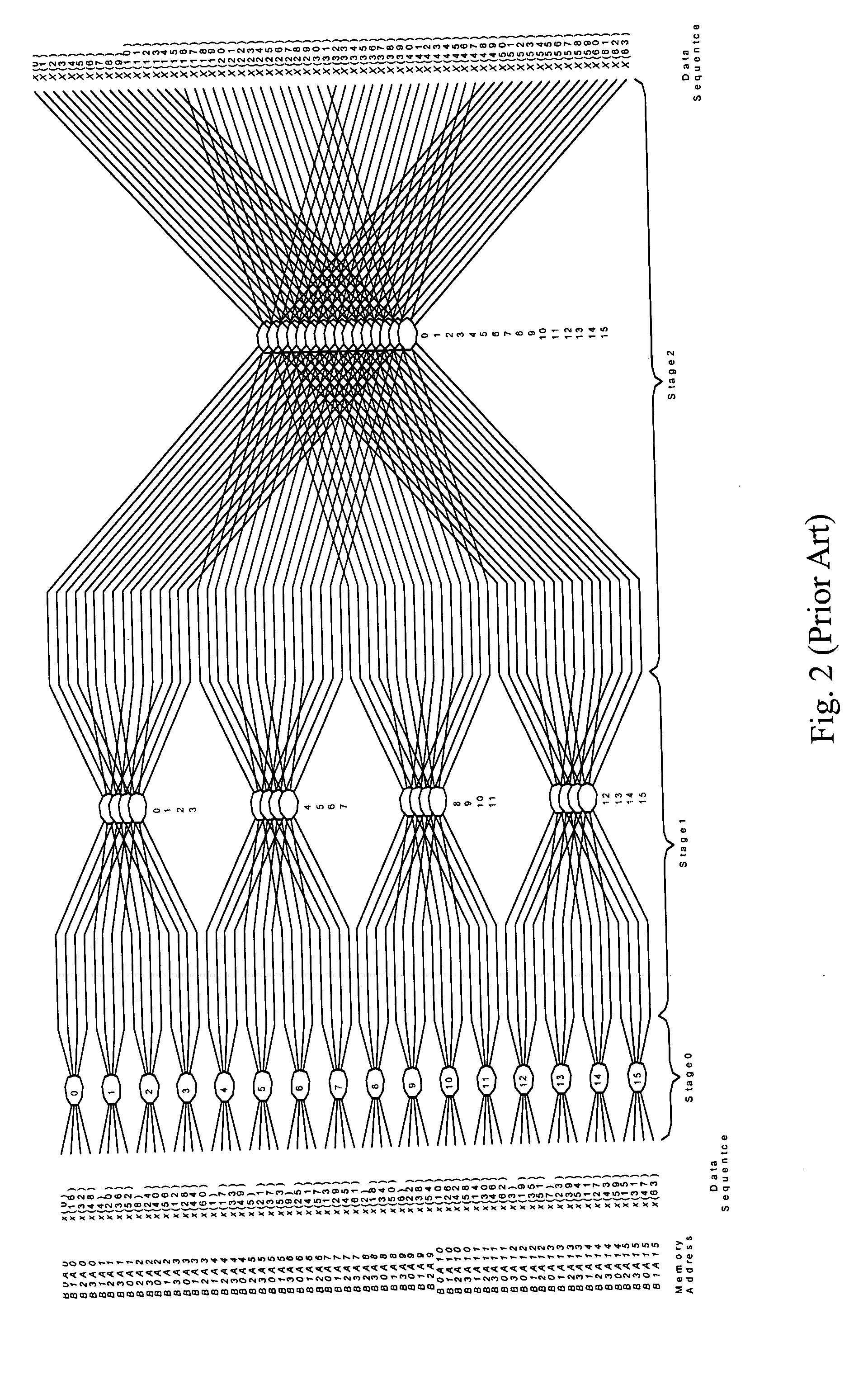
[0031] In this embodiment, the configuration of the present invention is the same with the traditional device 10 (N=64, r=4, R=3). However, the values of the configuration can be adjusted based on the demand of users.

[0032] As shown in FIG. 4, the FFT device 30 includes the processor 18, switches 32 and 34, memory units 36 and 38, an address controller 40, a sequence value modifier 42 and the sequence value generator 22, wherein the processor 18 and the sequence value generator 22 are identical to the prior processor and the sequence v...


PUM


Abstract

A memory-based Fast Fourier Transform device is provided, which adopts single-port random access memory (RAM), rather than dual-port RAM, as a storage, and the circuit area of the FFT device is therefore reduced. In order to enhance the access efficiency of the memory and the use efficiency of a processor, the transformer adopts a modified in-place conflict-free addressing to achieve similar performance of a traditional Fast Fourier Transform device.

Description

BACKGROUND OF THE INVENTION [0001] 1. Field of the Invention [0002] The invention relates to a Fast Fourier Transform (FFT) device and, more particularly, to a single-port RAM-based FFT device. [0003] 2. Description of Related Art [0004] FFT is a demodulating method commonly used in high-speed communication systems, and its corresponding modulating method is typically known as Inverse Fast Fourier Transform (IFFT). FFT is evolved from Discrete Fourier Transform (DFT). An N-point DFT can be represented by the following equation: X⁡(k)=∑n=0N-1⁢x⁡(n)⁢Wnnk,⁢for⁢ ⁢k=0,1,…⁢ ,N-1,⁢WNnk=ⅇ-j⁢2⁢π⁢ ⁢nkN.(1)[0005] However, equation (1) obviously implies the problem of high computational complexity to thus be replaced by FFT, which has a merit of lower computational complexity. FFT is widely used in high-speed communication systems. Here, a wide marketing broadband access technology, i.e., Asymmetric Digital Subscriber Line (ADSL), is given as a description of a high-speed communication system....

Claims


Application Information

Patent Timeline
IPC IPC(8): G06F17/14
CPCG06F17/142
Inventor YU, CHI-LI
Owner IND TECH RES INST
Why Eureka
Try Eureka