
Matching circuit

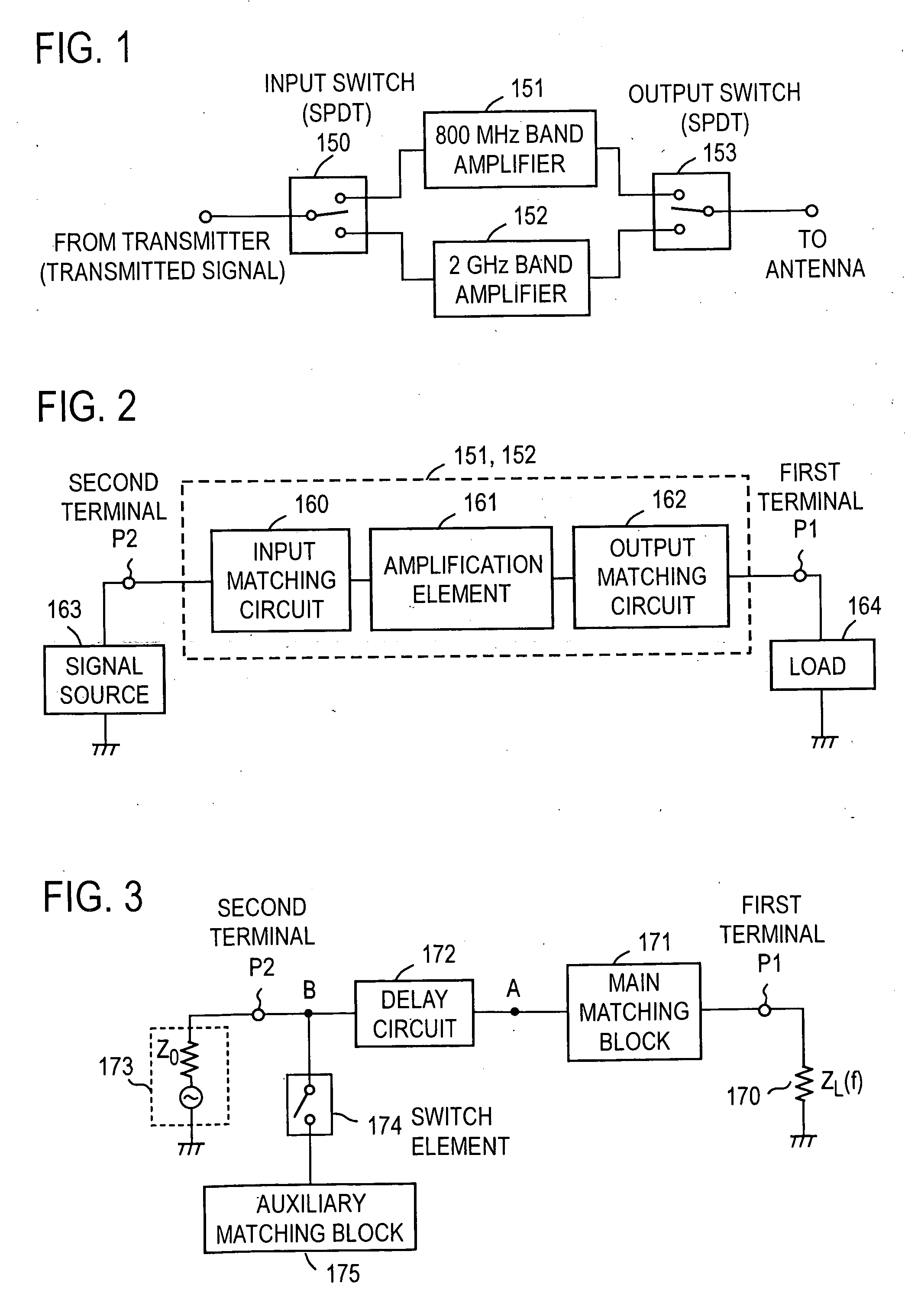
a matching circuit and circuit technology, applied in the field of matching circuits, can solve the problems of reducing gain and efficiency, increasing the total circuit area of the transmitter, and comparatively large components of transmission lines, and achieve the effect of small siz

Inactive Publication Date: 2006-11-23
NTT DOCOMO INC
View PDF2 Cites 35 Cited by
  • Summary
  • Abstract
  • Description
  • Claims
  • Application Information

AI Technical Summary

Benefits of technology

The present invention is a matching circuit that has two blocks: a first block and a second block. The second block matches the impedance of the signal source and the load in the lowest frequency band. The second block also has a π-type circuit for matching in high frequency bands. This configuration allows for better impedance matching in both low and high frequency bands. The second block is smaller than conventional matching circuits, making it easier to design and implement.

Problems solved by technology

Consequently, there has been the problem that the total circuit area of the transmitter became larger as the operating frequency bands rose.
However, compared to matching circuits designed for narrowband operation, the result is that there occurs a reduction in gain and efficiency.
However, particularly in cases where the frequency is low, transmission lines become comparatively large components inside the circuit.
However, in the case of transmission lines, the length easily becomes comparatively long.
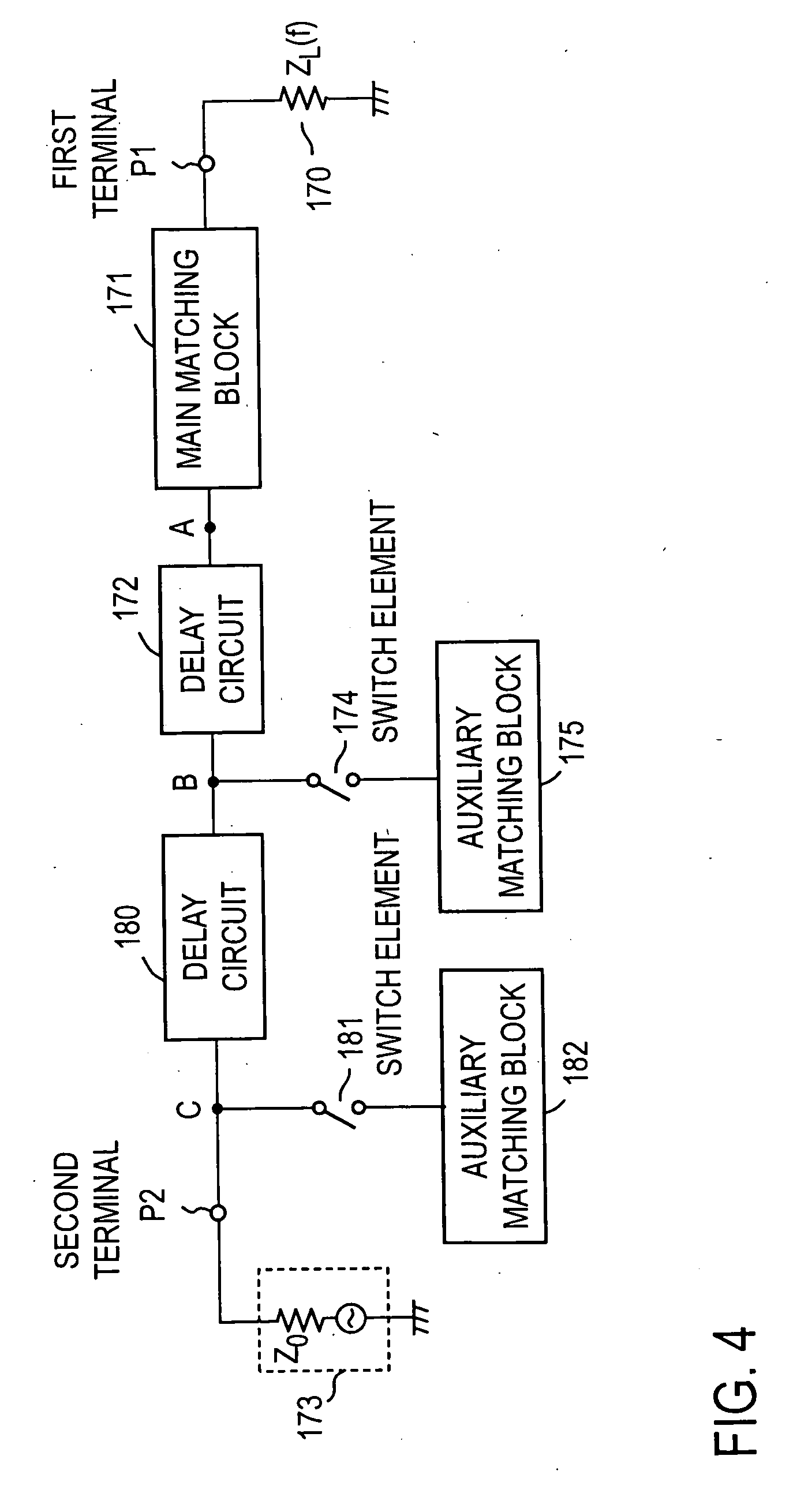
In particular, in the case where the used frequency is low, the area of a transmission line serving as a delay circuit becomes large, so there has been the problem that the matching circuit as a whole also was made bigger.
Further, this problem increases as the frequency becomes lower, and as the number of frequencies rises.

Method used


Image

  • Matching circuit
  • Matching circuit
  • Matching circuit

Examples


embodiment 1

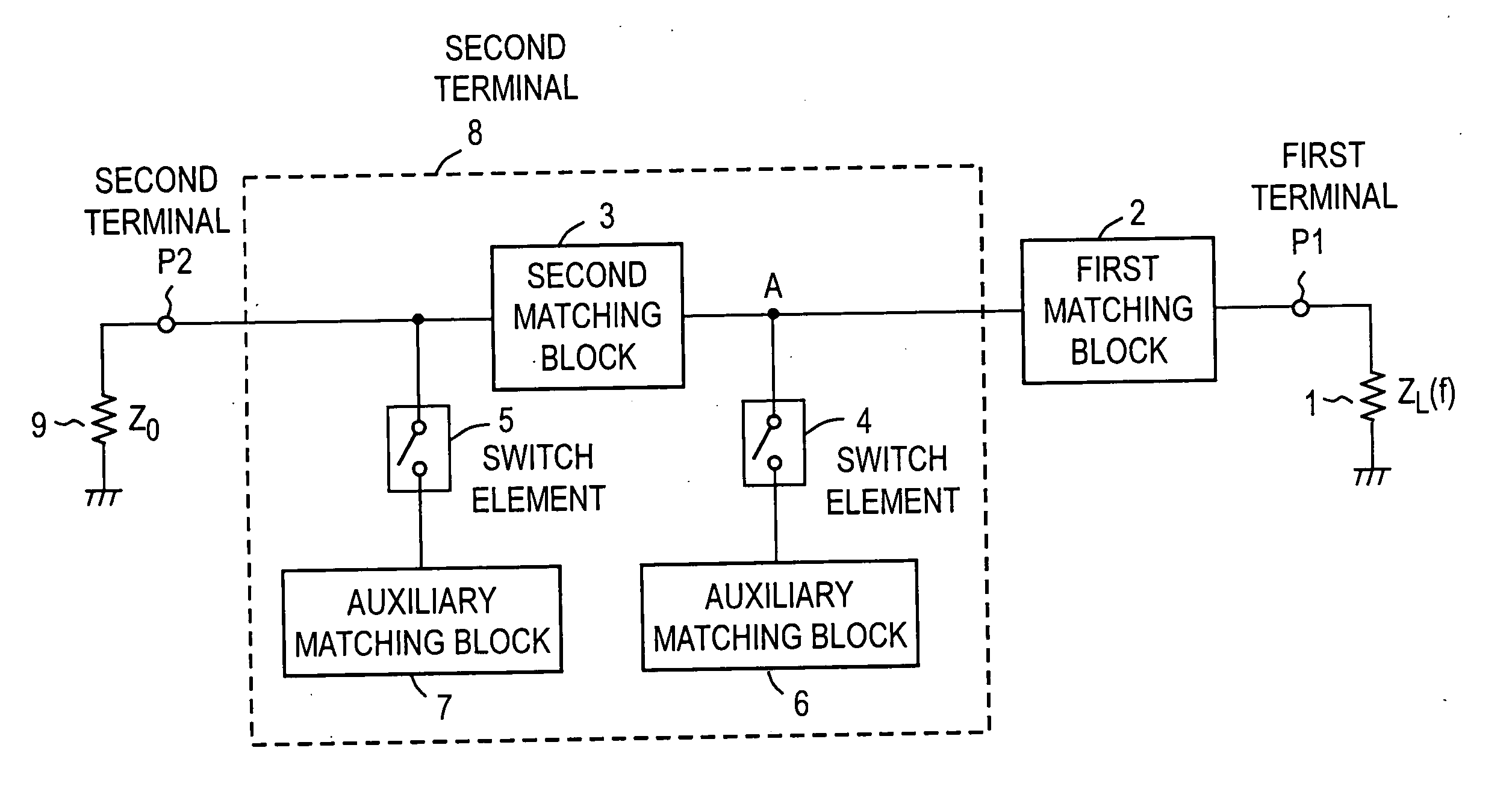
[0039] In FIG. 5, the basic configuration of a matching circuit of the present invention is shown. The matching circuit of the present invention is constituted by a first matching block 2 and a matching circuit part 8 consisting of lumped elements. Matching circuit part 8 is a π-type circuit constituted by a second matching block 3, switch elements 4 and 5, and auxiliary matching blocks 6 and 7. One end of first matching block 2 is connected to a first terminal P1 to which an element 1 (a load in this example) having an impedance ZL(f) with frequency-dependent characteristics is connected. To the other end of first matching block 2, one end of second matching block 3 is connected in series. The other end of second matching block 3 is connected, via a second terminal P2, to an element 9, e.g. a signal source, with an impedance Z0 whose impedance does not depend on the frequency. Also, to the terminal on the first matching block 2 side of second matching block 3, there is connected a ...

embodiment 2

[0045]FIG. 8 is an example where the basic structure of this invention, shown in FIG. 5, has been generalized so that it can be adapted to a plurality of frequency bands. This matching circuit is composed of first matching block 2, L-type blocks 43a to 43n, and shunt circuit blocks 46a to 46n. Each L-type block 43i (i=a to n) is composed of a second matching block 40i, a first switch element 41i, and a first auxiliary matching block 42i. One terminal of second matching block 40a is connected to first matching block 2. Also, the other end of second matching block 40a is connected to one terminal of second matching block 40b. In this way, each second matching block 40i is connected in series. First auxiliary matching block 42i is connected, via first switch element 41i, to the terminal of second matching block 40i on the side of first terminal P1. In other words, an L-type circuit is formed by means of second matching block 40i, first switch element 41i, and first auxiliary matching b...

embodiment 3

[0056] A matching circuit generalized by using π-type circuits was explained in FIG. 8, but it is also possible to configure a generalized matching circuit using T-type circuits. In FIG. 10, there is shown an embodiment of a matching circuit using two T-type circuits. This matching circuit is composed of first matching block 2, an L-type block part 63a, an L-type block part 63b, and a second matching block 60c. One end of first matching block 2 is connected to a first terminal P1 at which it is connected to element 1. Also, the other end of first matching block 2 is connected to one end of a second matching block 60a inside L-type block part 63a. To the other end of second matching block 60a, there is connected an auxiliary matching block 62a via a first switch element 61a. Moreover, the other end of second matching block 60a is also connected to one end of a second matching block 60b inside L-type block part 63b. To the other end of second matching block 60b, an auxiliary matching ...


PUM


Abstract

The present invention has for its object to provide a matching circuit with multiband capability which can be reduced in size, even if the number of handled frequency bands rises. The matching circuit of the present invention comprises a load having frequency-dependent characteristics, a first matching block connected with one end to the load with frequency-dependent characteristics, and a second matching block formed by lumped elements connected in series to the first matching block. And then, when a certain frequency band is used, matching is obtained with the series impedance of the first matching block and the second matching block. When a separate frequency band is used, a π-type circuit is constituted by connecting auxiliary matching blocks to both sides of the second matching block. Next, at the same frequency, by taking the combined impedance of this π-type circuit and a load whose characteristics do not depend on the frequency to be Z0, the influence of the second matching block is removed.

Description

BACKGROUND OF THE INVENTION [0001] 1. Field of the Invention [0002] This invention pertains to a matching circuit handling multiple bands which, in a plurality of frequency bands, establishes matching between circuits having different impedances. It pertains to matching circuits built into small-sized multiband power amplifiers which amplify, with high efficiency, signals in a plurality of frequency bands used e.g. in mobile communications and satellite communications. [0003] 2. Description of Related Art [0004] Accompanying the diversification of services offered by means of radio communications, conversion to multiband capability for processing signals in a plurality of frequency bands is required of radio equipment. As an indispensable device included in radio equipment, there is the power amplifier. In order to carry out efficient amplification, there is a need to obtain impedance matching between the amplification element and its peripheral circuits, so a matching circuit is us...

Claims


Application Information

Patent Timeline
Patent Type & Authority Applications(United States)
IPC IPC(8): H03H7/38
CPCH04B1/0458H03H7/383H04B1/44
Inventor FUKUDA, ATSUSHIOKAZAKI, HIROSHINARAHASHI, SHOICHI
Owner NTT DOCOMO INC
Learn More