Field blooming color filter layer for displays

a color filter layer and field-blooming technology, applied in the field of display sheets, can solve the problems of heavy and expensive electric display, and achieve the effect of little effect on drive voltag

Inactive Publication Date: 2006-11-23
IND TECH RES INST
View PDF16 Cites 8 Cited by
  • Summary
  • Abstract
  • Description
  • Claims
  • Application Information

AI Technical Summary

Benefits of technology

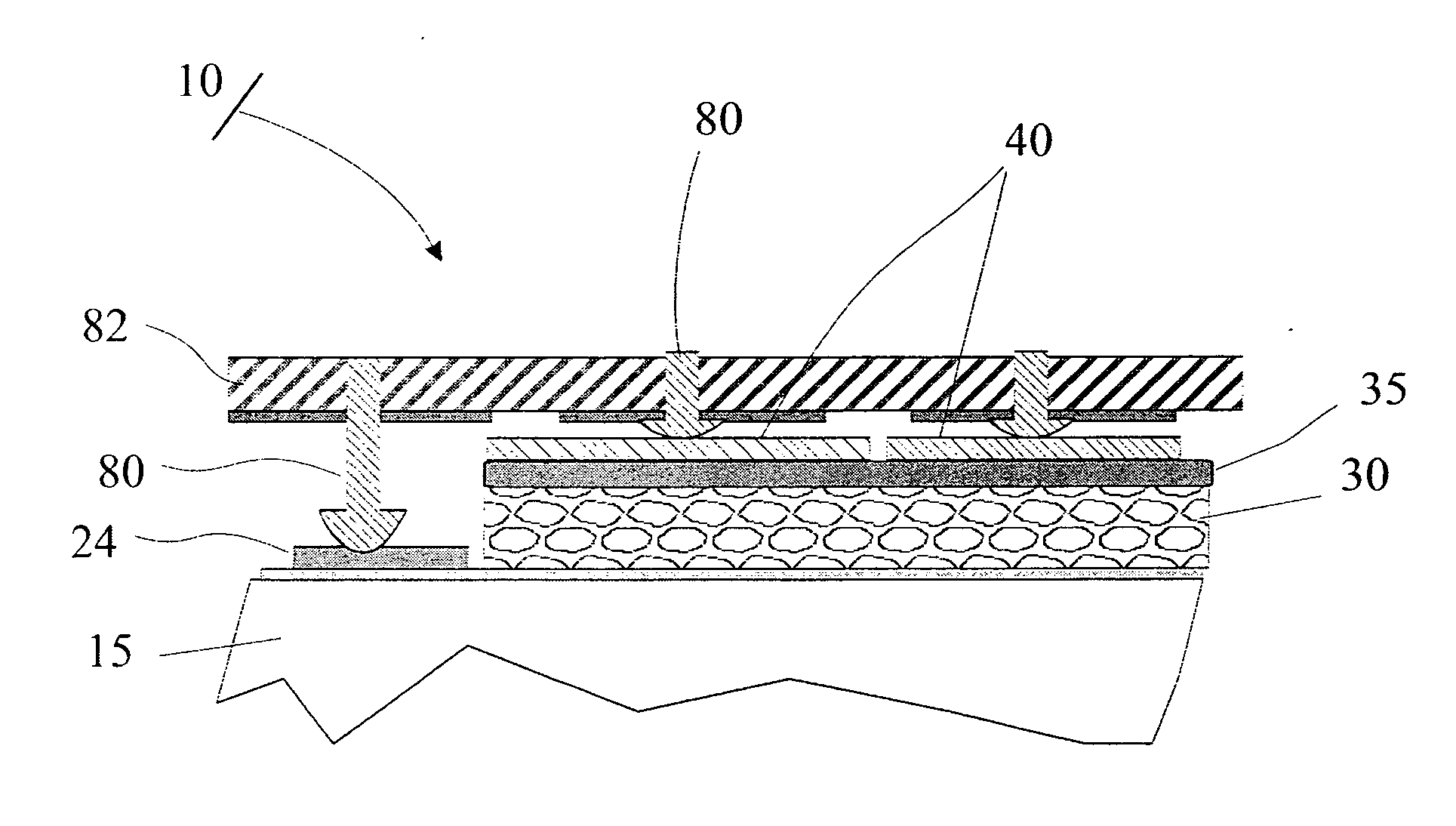
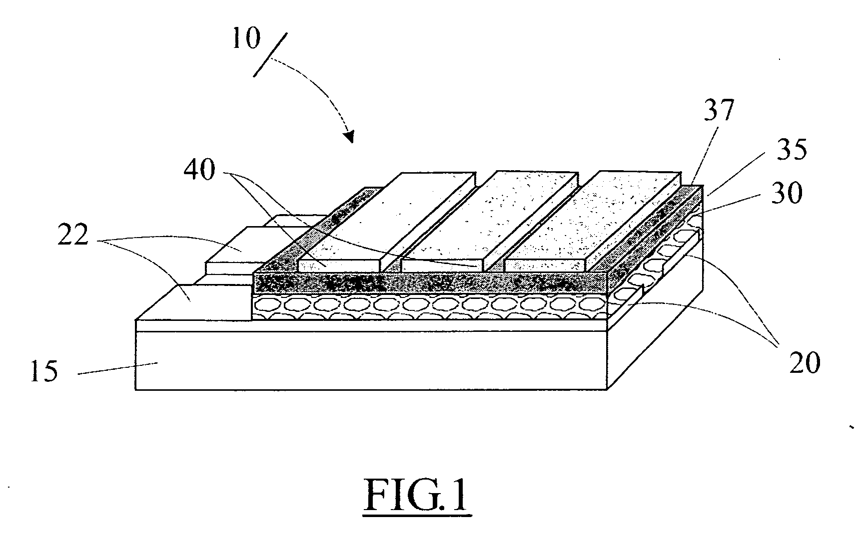
[0012] The present invention includes several advantages, not all of which are incorporated in a single embodiment. This invention provides a field blooming color filter layer for cholesteric displays. The field blooming color filter layer may optionally operate in conjunction with a reflective surface to provide complementary light in a polymer dispersed cholesteric display.
[0013] The present invention provides a bri

Problems solved by technology

Electrically updated displa

Method used


Image

  • Field blooming color filter layer for displays
  • Field blooming color filter layer for displays
  • Field blooming color filter layer for displays

Examples


example 1

Comparative

[0052] An experiment was performed to determine the optical properties and electrical properties of a submicron indium-tin-oxide powder, 95 / 5 CITOH “C” from Umicore Indium Products, Providence, R.I. The material, hereafter known as ITO powder, was dispersed in water according to the following formula

5.00 gms.ITO powder50.00 gms. Deionized water0.10 gms.Surfynol 131 dispersing agent

[0053] The ITO powder was dispersed using 6 minutes of energy from a Branson Digital Sonifier, Model 450. Kodak deionized photographic gelatin was melted into the solution in the form of 5 grams of swollen gel, having a 40% dried gelatin content, hereafter known as “swollen gel”. Three drops of a surfactant, Zonyl FSO, was added to permit the mixture to be wet-coated in thin layers. The mixture was coated at 25 cc per meter over a plastic substrate. The dried film was highly conductive, having a conductivity of 50-200 ohms per square. The film was slightly translucent, but functionally transp...

example 2

Comparison

[0054] The invention requires a nonconductive layer, and a series of mixtures having progressively less ITO powder were made according to the processes in Example 1 until the following mixture proved to be nonconductive:

1.70 gms.Submicron Indium-Tin-Oxide powder;Umicore Indium Products 95 / 5 CITOH “C”50.00 gms. Deionized water0.10 gms.Surfynol 131 dispersing agent5.00 gms swollen gel

example 3

Comparative

[0055] A complementary dye solution appropriate for use with a yellow cholesteric layer to form a color-neutral display was created. Two pigments were used, Sunfast Blue 15:4 milled to a 110 nanometer mean diameter, hereafter known as Kodak cyan, and Pigment violet 29 milled to a 210 nanometer mean diameter, hereafter known as Kodak magenta. Both materials were suspended in water at a 12% concentration.

[0056] The following solution provided a non-field blooming color filter layer:

1.00 gms.Kodak cyan, 12% concentration2.00 gms Kodak magenta, 12% concentration2.80 gms Kodak gelatin, 40% concentration44.2 gms.Deionized water

The solution was coated over clear plastic at 10.76 grams per square meter and dried. The reflective density for the layer were: Red 2.63, Green 2.77, Blue 1.03.


PUM

PropertyMeasurementUnit
Lengthaaaaaaaaaa
Nanoscale particle sizeaaaaaaaaaa

Abstract

The present invention relates to a display sheet comprising a substrate for carrying layers of material, an imaging layer comprising a bistable polymer dispersed cholesteric liquid crystal imaging layer, a first patterned transparent conductor disposed on one side of the bistable polymer dispersed cholesteric liquid crystal imaging layer, a field blooming color filter layer, and a second patterned electrode on the side of the bistable polymer dispersed cholesteric liquid crystal imaging layer opposite the first patterned conductor and a method for making the same.

Description

CROSS REFERENCE TO RELATED APPLICATIONS [0001] Reference is made to commonly assigned, co-pending U.S. patent applications: Ser. No. ______ by Burberry et al. (Docket 89357) filed of even date herewith entitled “Reflective Layer Field Blooming Layer For LC Display”; Ser. No. ______ by Burberry et al. (Docket 89431) filed of even date herewith entitled “Controlled GAP States For Liquid Crystal Displays”; and Ser. No. ______ by Burberry et al. (Docket 90600) filed of even date herewith entitled “Conductive Layer To Reduce Drive Voltage In Displays”, incorporated herein by reference.FIELD OF THE INVENTION [0002] The present invention relates to a display sheet having a cholesteric liquid layer that can change states to provide a viewable image. BACKGROUND OF THE INVENTION [0003] Currently, information is displayed using assembled sheets of paper carrying permanent inks or displayed on electronically modulated surfaces such as cathode ray displays or liquid crystal displays. Printed ...

Claims


Application Information

Patent Timeline
IPC IPC(8): G02F1/1333
CPCG02F1/1334G02F1/133514G02F2001/13775G02F1/13718G02F1/133707G02F1/13775
Inventor STEPHENSON, STANLEY W. III
Owner IND TECH RES INST
Why Eureka
Try Eureka