Fused Polycyclic Compound, and Preparation Method and Use Thereof
a polycyclic compound and polycyclic compound technology, applied in the field of display technologies, can solve the problems of reducing the performance and luminescence efficiency of oled devices, affecting the lifetime and luminescence efficiency of devices, etc., and achieve the effects of reducing exciton loss, promoting förster energy transfer, and suppressing dexter energy transfer
- Summary
- Abstract
- Description
- Claims
- Application Information
AI Technical Summary
Benefits of technology
Problems solved by technology
Method used
Image
Examples
example 1
Device Example 1
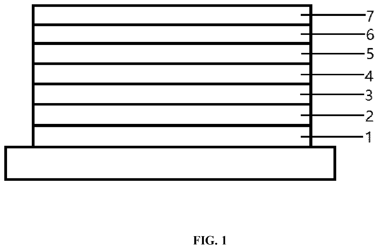
[0155]This example provides an organic light-emitting device, which includes, from bottom to top, an anode 1, a hole injection layer 2, a hole transport layer 3, a light emitting layer 4, an electron transport layer 5, an electron injection layer 6 and a cathode 7 stacked in sequence. The device is configured to have a particular structure of ITO / hole injection layer (HIL) (30 nm) / hole transport layer (HTL) (40 nm) / organic light-emitting layer (compound 10 doped with compound RD) (40 nm) / electron transport layer (ETL) (40 nm) / electron injection layer (EIL / LiF) (1 nm) / cathode (Al) (150 nm) as shown in FIG. 1.
[0156]In the organic light-emitting device, the material of the anode 1 is ITO.
[0157]The material of the hole injection layer 2 is the compound HAT(CN)6 having a structure below:
[0158]The material of the hole transport layer 3 is the compound NPB having a structure below:
[0159]The organic light emitting layer 4 is formed by blending a host material and a guest mat...
example 2
Device Example 2
[0173]This example provides an organic light-emitting device, which differs from the organic light-emitting device provided in Device Example 1 in that the host material in the light emitting layer is the compound 11.
example 3
Device Example 3
[0174]This example provides an organic light-emitting device, which differs from the organic light-emitting device provided in Device Example 1 in that the host material in the light emitting layer is the compound 14.
PUM
| Property | Measurement | Unit |
|---|---|---|
| temperature | aaaaa | aaaaa |
| temperature | aaaaa | aaaaa |
| temperature | aaaaa | aaaaa |
Abstract
Description
Claims
Application Information


