

Organic Electroluminescent Device
an electroluminescent device and organic technology, applied in the direction of luminescent compositions, thermoelectric devices, organic chemistry, etc., can solve the problems of excessive holes flowing out to the side of the electron-transporting layer, failure to emit light at high efficiency, and no means, etc., to achieve good injection and transportation characteristics of holes and electrons, low driving voltage, and high durability
- Summary
- Abstract
- Description
- Claims
- Application Information
AI Technical Summary
Benefits of technology
Problems solved by technology
Method used
Image

Examples
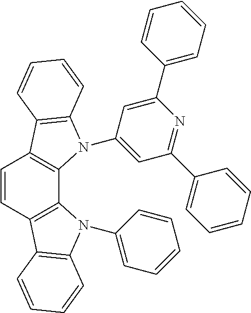
synthetic example 1
Synthesis of Compound 1
[0093]
[0094]Under a nitrogen atmosphere, 100 ml of dehydrated N,N-dimethylformamide (DMF) was added to 2.52 g (0.059 mol) of sodium hydride (56.4% dispersion) and stirred. To 10.0 g (0.024 mol) of 5,7-dihydro-6-phenyl-diindolo[2,3-a:3′,2′-i]carbazole was added 100 ml of DMF while allowing dissolution to occur and the resulting solution was added dropwise to the above mixture over 30 minutes. After completion of the dropwise addition, the stirring was continued at room temperature for 1 hour. Then, 100 ml of DMF was added to 13.97 g (0.052 mol) of 2-chloro-4,6-diphenyl-1,3,5-triazine while allowing dissolution to occur and the resulting solution was added dropwise to the above mixture over 30 minutes. After completion of the dropwise addition, the stirring was continued for 7 hours. Thereafter, the stirring was continued at 80 ° C. for 15 hours. The reaction mixture was cooled to room temperature, 300 ml of water was added, and the precipitated crystal was coll...
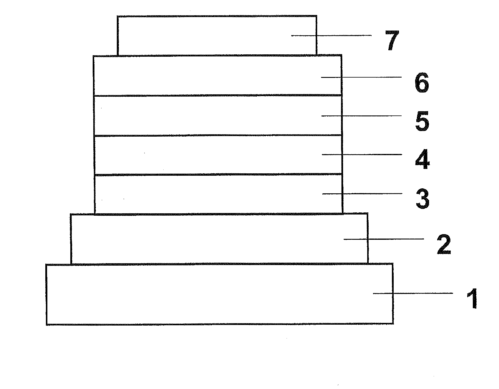
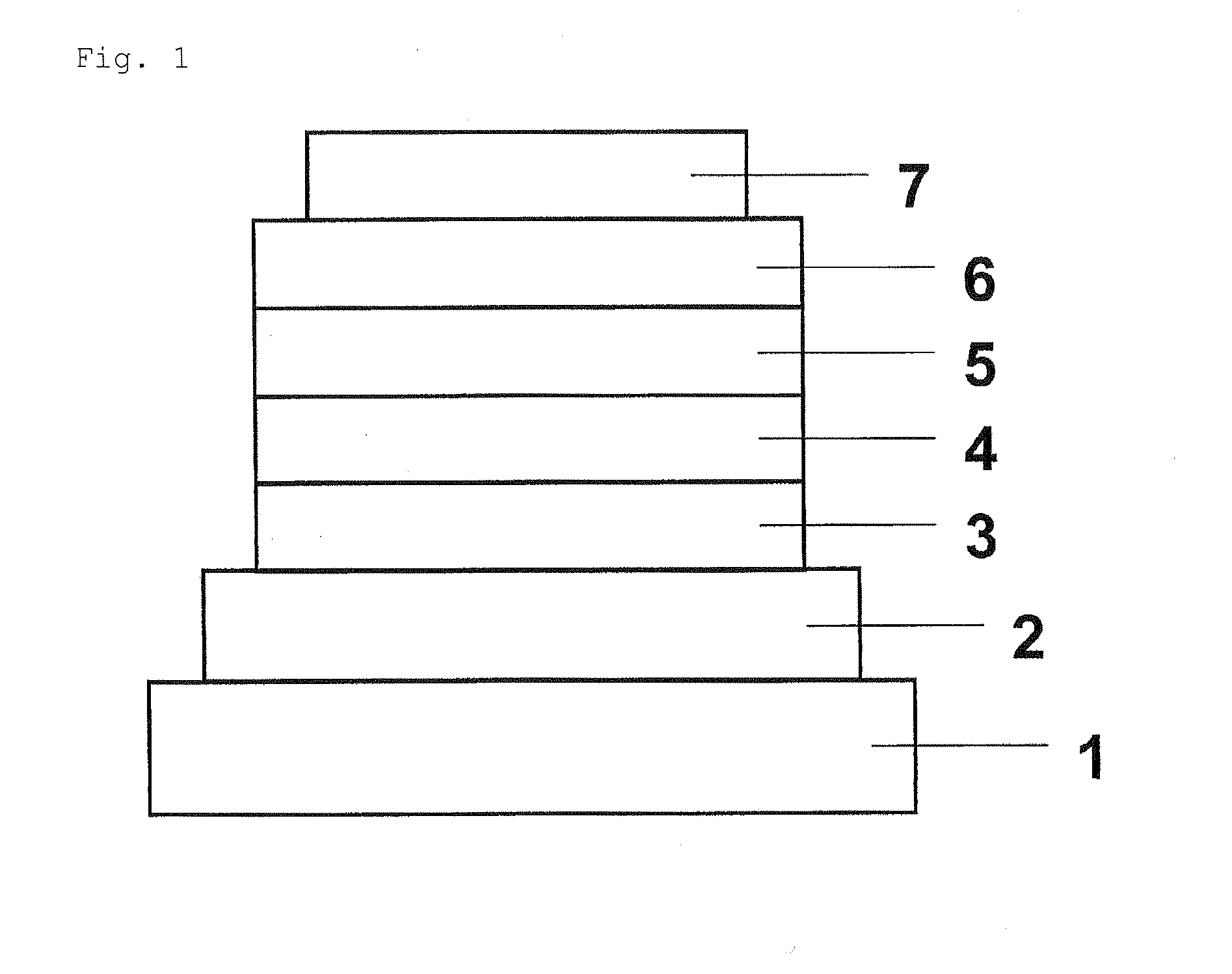
example 1
[0096]The constituent layers were deposited in thin film by the vacuum deposition process at a degree of vacuum of 4.0×10⁻⁵ Pa one upon another on a glass substrate on which a 110 nm-thick ITO anode had been formed. First, copper phthalocyanine (CuPC) was deposited on the ITO anode to a thickness of 25 nm. Then, 4,4′-bis[N-(1-naphthyl)-N-phenylamino]biphenyl (NPB) was deposited to a thickness of 40 nm to form a hole-transporting layer. Next, Compound 1 obtained in Synthetic Example 1 as a host material and tris(2-phenylpyridine)iridium (III) (Ir(ppy)3) as a phosphorescent dopant were co-deposited on the hole-transporting layer from different deposition sources to a thickness of 40 nm to form a light-emitting layer. The concentration of Ir(ppy)3 in the light-emitting layer was 10.0 wt %. Next, tris(8-hydroxyquinolinato)aluminum (III) (Alq3) was deposited to a thickness of 20 nm to form an electron-transporting layer. Further, lithium fluoride (LiF) was deposited on the electron-trans...
example 2
[0100]The constituent layers were deposited in thin film by the vacuum deposition process at a degree of vacuum of 4.0×10⁻⁴ Pa one upon another on a glass substrate on which a 150 nm-thick ITO anode had been formed. First, copper phthalocyanine (CuPC) was deposited on the ITO anode to a thickness of 25 nm to form a hole-injecting layer. Then, NPB was deposited on the hole-injecting layer to a thickness of 55 nm to form a hole-transporting layer. Next, Compound 24 as a host material and bis(2-(2′-benzo[4,5-a]thienyl)pyridinato-N, C3]iridium(acetylacetonate) ((Btp)2Iracac) were co-deposited on the hole-transporting layer from different deposition sources to a thickness of 47.5 nm to form a light-emitting layer. At this time, the concentration of (Btp)2Iracac was 8.0 wt %. Next, Alq3 was deposited to a thickness of 30 nm to form an electron-transporting layer. Further, LiF was deposited on the electron-transporting layer to a thickness of 1 nm to form an electron-injecting layer. Final...
PUM
 Abstract
Description
Claims
Application Information