Negative resistance field-effect element

a field-effect element and negative resistance technology, applied in the field of field-effect elements, can solve the problems of unsuitable logic element and integrated element application, lack of control terminal itself, and inability to anticipate amplification capability or the lik

Inactive Publication Date: 2006-11-30
NAT INST OF ADVANCED IND SCI & TECH +1
View PDF2 Cites 15 Cited by
  • Summary
  • Abstract
  • Description
  • Claims
  • Application Information

AI Technical Summary

Problems solved by technology

Although a so-called two-terminal element having no control terminal exists, the lack of a control terminal itself tends to be a drawback, limiting control from the outside and usually making the element unsuitable for application as a logic element and as an integrated element.
Naturally, no amplification capability or the like can be anticipated.
Howev

Method used


Image

  • Negative resistance field-effect element
  • Negative resistance field-effect element
  • Negative resistance field-effect element

Examples


Embodiment Construction

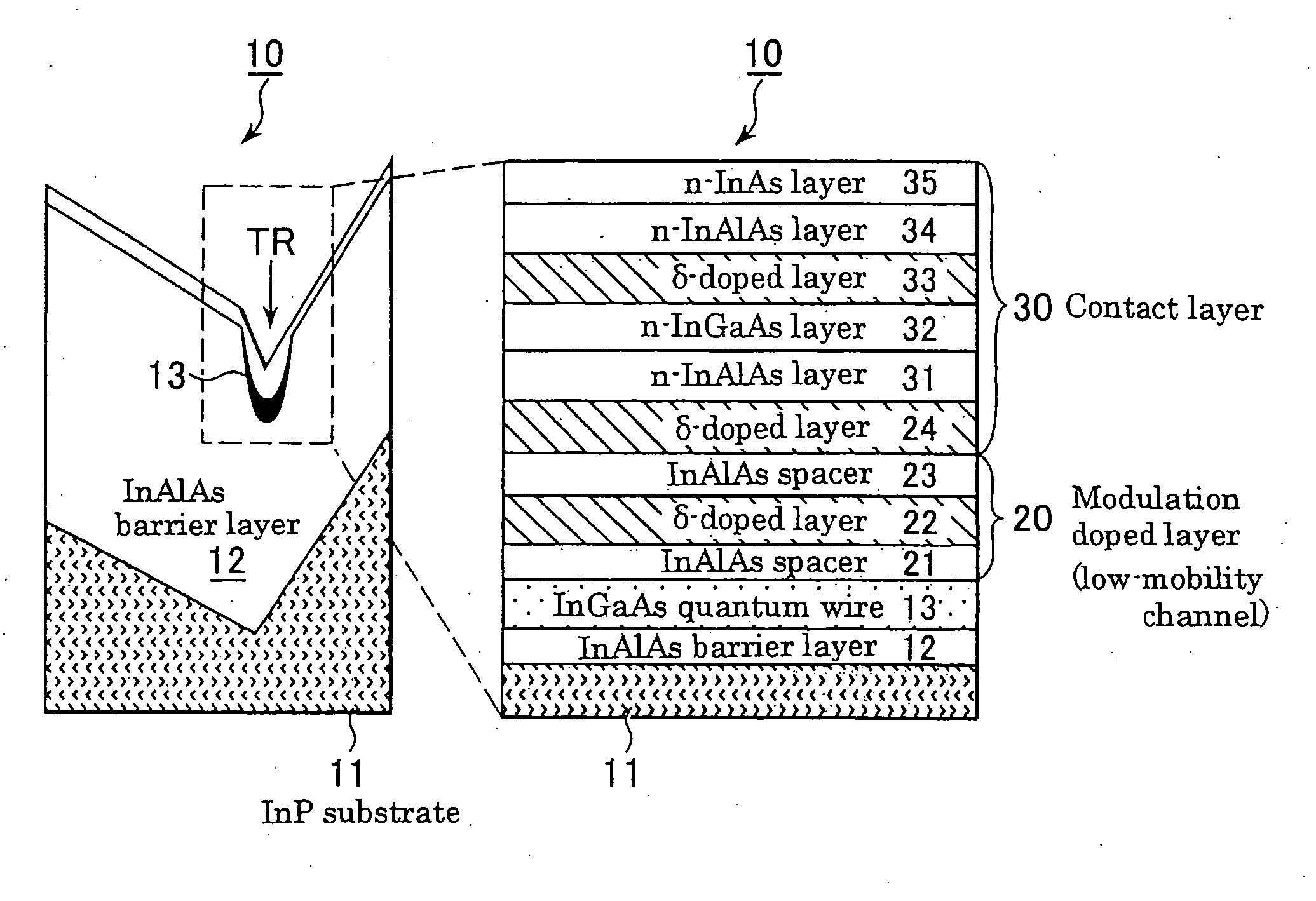
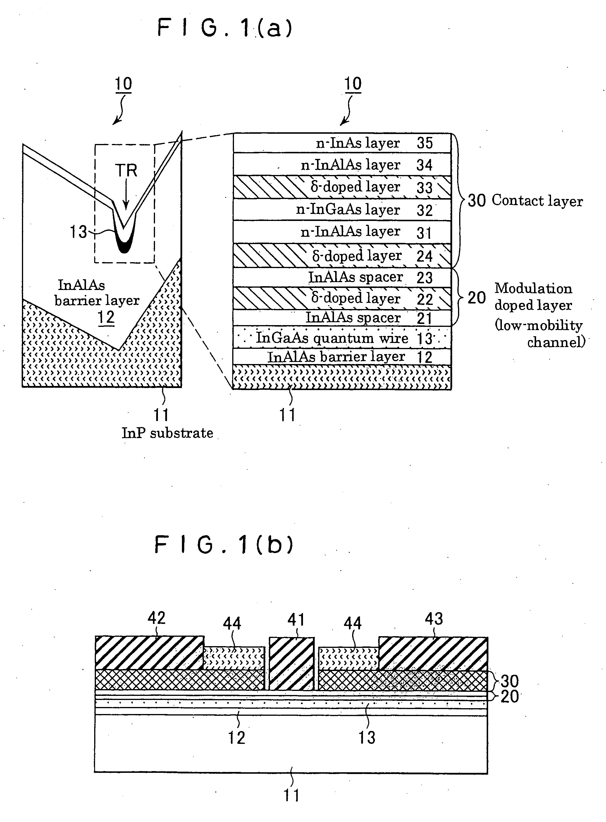
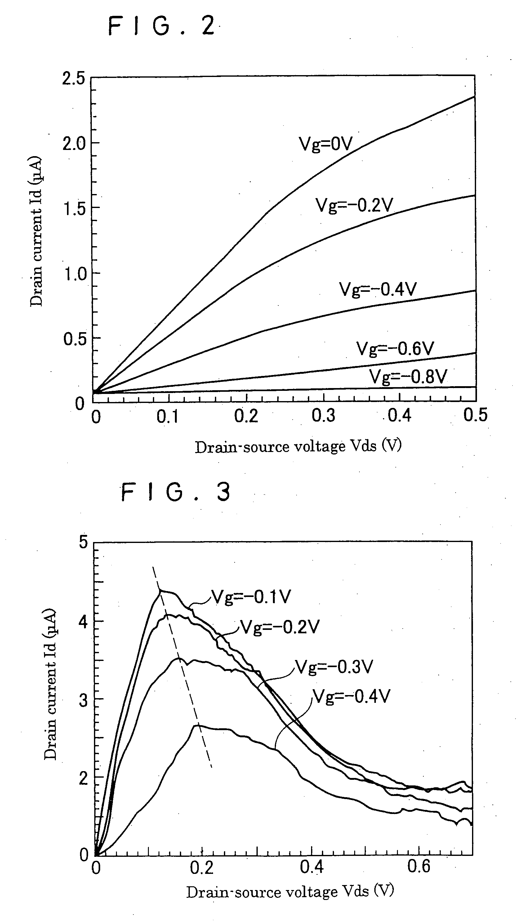
[0017] A preferred embodiment of a negative resistance field-effect element 10 configured according to the present invention is shown in FIGS. 1(A) and (B). As viewed statically from the sectional structure shown in the left-side diagram of FIG. 1(A), an InAlAs or AlGaAs barrier layer, in this case an InAlAs barrier layer 12, is formed on an InP or GaAs substrate, in the illustrated case an InP substrate 11, having an asymmetrical V-groove, thereby forming a trench TR that is a deep V-groove having very steep lateral faces at the location of the InAlAs barrier layer 12 where the V-groove is present in the underlying InP substrate 11. The distance between the inclined surfaces near the bottom portion of the trench TR (space width) can, as explained later, be formed very narrowly.

[0018] Details of the sectional lamination at the essential portion enclosed by the phantom line in the left-side diagram are shown in the right-side diagram of FIG. 1(A). Referring to this, first an InGaAs ...


PUM


Abstract

A negative resistance field-effect element that is a negative differential resistance field-effect element capable of achieving negative resistance at a low power supply voltage (low drain voltage) and also enabling securement of a high PVCR is formed on its InP substrate 11 having an asymmetrical V-groove whose surface on one side is a (100) plane and surface on the other side is a (011) plane with an InAlAs barrier layer (12) that has a trench (TR) one of whose opposed lateral faces is a (111) A plane and the other of which is a (331) B plane. An InGaAs quantum wire (13) that has a relatively narrow energy band gap is formed at the trench bottom surface as a high-mobility channel. An InAlAs modulation-doped layer (20) having a relatively wide energy band gap is formed on the quantum wire as a low-mobility channel. A source electrode (42) and a drain electrode (43) each in electrical continuity with the quantum wire (13) constituting the high-mobility channel through a contact layer (30) and extending in the longitudinal direction of the quantum wire (13) as spaced from each other, and a gate electrode (41) provided between the source electrode (42) and the drain electrode (43) to face the low-mobility channel (20) through an insulating layer or a Schottky junction, are provided. Owing to the foregoing configuration, a very narrow-width quantum wire whose lateral confinement size can, without restriction by the lithographic technology limit, be made 100 nm or less is usable as a high-mobility channel, whereby there can be obtained a negative resistance field-effect element that develops a negative characteristic at a low power supply voltage and enables securement of a high PVCR.

Description

TECHNICAL FIELD [0001] The present invention relates to a field-effect element that exhibits negative differential resistance (NDR) and more particularly relates to an improvement for enhancing a peak-to-valley current ratio (hereinafter abbreviated as PVCR), which, being the ratio between drain current value immediately before negative differential resistance is exhibited and drain current value immediately after occurrence of negative differential resistance, is an index for measuring negative differential resistance effect, and, further, for enabling the field-effect element to exhibit a negative characteristic at a low power supply voltage. In this description, a field-effect element that exhibits negative differential resistance will, in accordance with general practice, be called simply a negative resistance field-effect element. BACKGROUND ART [0002] Elements having negative differential resistance are required in semiconductor integrated circuits. As with other active elemen...

Claims


Application Information

Patent Timeline
IPC IPC(8): H01L31/00H01L29/872H01L21/338H01L29/04H01L29/06H01L29/12H01L29/417H01L29/47H01L29/775H01L29/80H01L29/812
CPCB82Y10/00H01L29/775H01L29/125H01L29/045
Inventor OGURA, MUTSUOSUGAYA, TAKEYOSHIJANG, KEE-YOUNSUGIYAMA, YOSHINOBU
Owner NAT INST OF ADVANCED IND SCI & TECH
Why Eureka
Try Eureka