Organic light emitting display

a light-emitting display and organic technology, applied in the field of organic light-emitting displays, can solve the problems of high response speed of about 1 s, increased cost of production, and consumption of low power, and achieve the effect of uniform luminance and reduced number of data drivers

Active Publication Date: 2006-11-30
SAMSUNG DISPLAY CO LTD
View PDF15 Cites 116 Cited by
  • Summary
  • Abstract
  • Description
  • Claims
  • Application Information

AI Technical Summary

Benefits of technology

[0014] The present invention, therefore, provides an organic light emitting display (OLED), which makes use of demultiplexers to decrease the number of data drivers and display an image having uniform luminance.

Problems solved by technology

The OLED has a high response speed of about 1 μs and consumes low power.
Thus, the cost of production further increases.

Method used


Image

  • Organic light emitting display
  • Organic light emitting display
  • Organic light emitting display

Examples


second embodiment

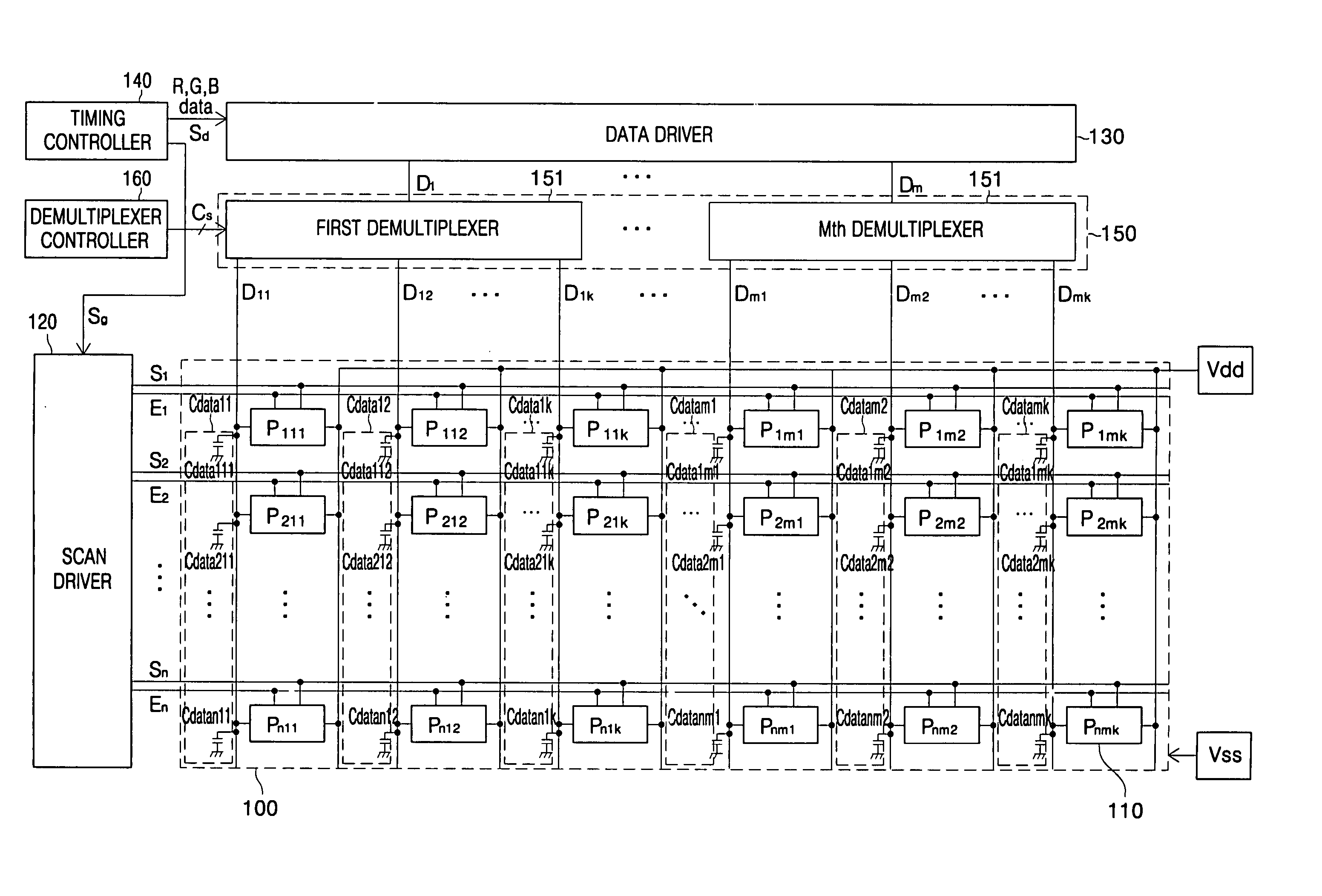
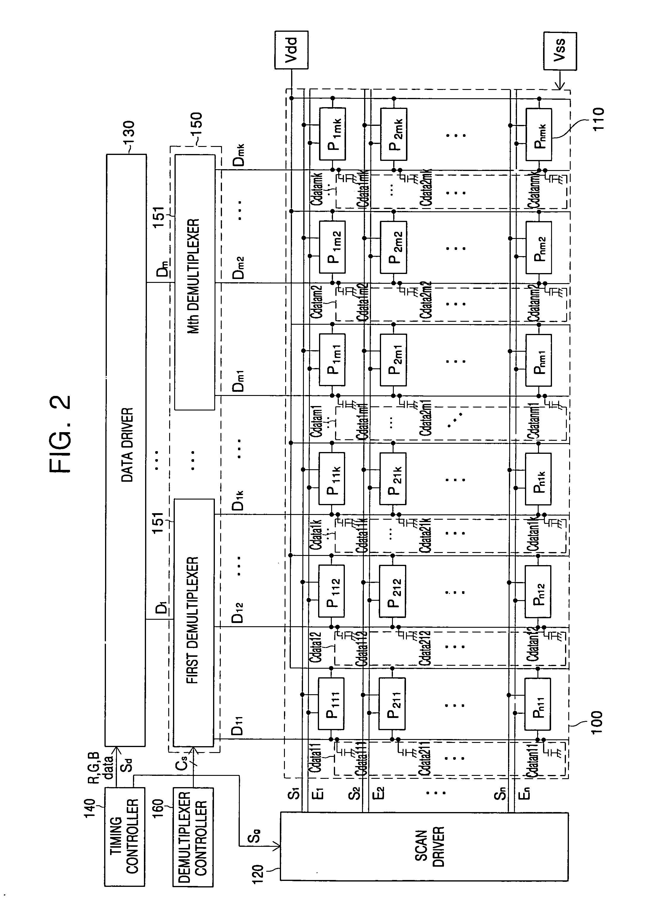
[0119] Accordingly, the data line capacitor Cdata has a structure to which the first and second data line capacitors Cdata1 and Cdata2 are connected in parallel about the data line 225. That is, Cdata=Cdata1+Cdata2. In applying the pixel structure according to the present invention, the data line capacitor Cdata has a capacitance of 20 to 50[PF], which is about 16 times more than in the conventional pixel structure. Therefore, when the pixel driving method using the demultiplexers is used, the gate voltage Vg of a driving transistor becomes substantially equal to the applied data voltage Vdata, so that the OLED can display exact gray scale and have uniform luminance.

[0120] The capacitance of the data line capacitor Cdata may be adjusted by controlling the size of a via hole formed in an insulating layer, such as a passivation layer, a planarization layer, or a PDL and the size of a contact hole via which a semiconductor layer is in contact with a metal layer.

[0121]FIG. 10 is a cros...

third embodiment

[0136] Accordingly, the data line capacitor Cdata has a structure to which the first and second data line capacitors Cdata1 and Cdata2 are connected in parallel about the data line 225. That is, Cdata=Cdata1+Cdata2. In applying the pixel structure according to the present invention, the data line capacitor Cdata has a capacitance of 20 to 50[PF], which is about 16 times more than in the conventional pixel structure. Therefore, when the pixel driving method using the demultiplexers is used, the gate voltage Vg of a driving transistor becomes substantially equal to the applied data voltage Vdata, so that the OLED can display exact gray scale and have uniform luminance.

[0137] The capacitance of the data line capacitor Cdata may be adjusted by controlling the size of a via hole formed in an insulating layer, such as a passivation layer, a planarization layer, or a PDL and the size of a contact hole via which a semiconductor layer is in contact with a metal layer.

[0138]FIG. 11 is a cros...

fourth embodiment

[0154] Accordingly, the data line capacitor Cdata has a structure to which the first and second data line capacitors Cdata1 and Cdata2 are connected in parallel about the data line 225. That is, Cdata=Cdata1+Cdata2. In applying the pixel structure according to the present invention, the data line capacitor Cdata has a capacitance of 20 to 50[PF], which is about 16 times more than in the conventional pixel structure. Therefore, when the pixel driving method using the demultiplexers is used, the gate voltage Vg of a driving transistor becomes substantially equal to the applied data voltage Vdata, so that the OLED can display exact gray scale and have uniform luminance.

[0155] The capacitance of the data line capacitor Cdata may be selected by controlling the size of a via hole formed in an insulating layer, such as a passivation layer, a planarization layer, or a PDL and the size of a contact hole via which a semiconductor layer is in contact with a metal layer.

[0156]FIG. 12 is a circ...


PUM


Abstract

An organic light emitting display (OLED) is provided. The OLED includes data line capacitors, which is disposed in a plurality of data lines included in a display panel. Each of the data line capacitors has a larger capacitance than a storage capacitor of each pixel. The data line capacitor includes the data line, an insulating layer, a metal, which are stacked. The metal is a cathode or a pixel electrode. The insulating layer of the data line capacitor is a passivation layer, a planarization layer, or a pixel defining layer. The capacitance of the data line capacitor is adjusted by controlling the thickness of the insulating layer or controlling the size of a via hole or a contact hole for controlling the thickness of the insulating layer.

Description

CROSS-REFERENCE TO RELATED APPLICATIONS [0001] This application claims priority to and the benefit of Korean Patent Application No. 10-2005-0039895, filed May 12, 2005, which is incorporated herein by reference in its entirety. BACKGROUND OF THE INVENTION [0002] 1. Field of the Invention [0003] The present invention relates to an organic light emitting display (OLED), and more particularly, to an OLED that makes use of demultiplexers to decrease the number of output lines of data drivers and display an image having uniform luminance. [0004] 2. Description of the Related Art [0005] In recent years, a variety of flat panel displays (FPDs) with small weight and volume have been developed to overcome the drawbacks of a cathode ray tube (CRT). The FPDs can be categorized into a liquid crystal display (LCD), a field emission display (FED), a plasma display panel (PDP), an organic light emitting display (OLED), and the like. [0006] An OLED includes an organic light emitting diode, which is...

Claims


Application Information

Patent Timeline
Patent Type & Authority Applications(United States)
IPC IPC(8): G09G3/30
CPCG09G3/3233G09G2300/0819G09G2300/0842H01L27/3244G09G2300/0861G09G2310/0297G09G2320/043G09G2300/0852H10K59/1216H10K59/12H10K50/818G09G3/30
Inventor KWAK, WON-KYUKIM, YANG-WAN
Owner SAMSUNG DISPLAY CO LTD
Why Eureka
Try Eureka