Flash storage

a technology of flash storage and storage media, applied in the field of flash storage, can solve the problems of inconsistency between the physical memory block and the replacement data, and achieve the effects of reducing the time of data access, reducing the cost of storage, and prolonging the service life of the control memory block

Inactive Publication Date: 2006-11-30
PROLIFIC TECH INC
View PDF2 Cites 31 Cited by
  • Summary
  • Abstract
  • Description
  • Claims
  • Application Information

AI Technical Summary

Benefits of technology

[0013] Accordingly, it is the primary object of the present invention to provide a flash storage, which is mainly provided with a logical address pointer column in each physical sector, allowing to write physical data together with a logical address pointer data into the physical sector simultaneously, in such a way that a plurality of logical pointer data may be presented in the same physical memory block, whereby the safety and reliability in data access may be ensured.
[0020] It is another object of the present invention to provide a flash storage, in which, mainly, the rising edge or falling edge of the system clock may be used by the micro-controller as a basis for data access signal, for thereby achieving the effect of adjustment of internal frequency and electrical power-saving.

Problems solved by technology

Writing data into the replacement data of the physical memory block may be allowable only when the data accessing operation is completed, and there is no consistency between the physical memory block and the replacement data so as to produce damage in accessed data if an abnormal behavior, such as power failure and so on, occurs at this time.
The change in the data access signal of the micro-controller should occur at the rising edges of the system clock only, in such a way that the timely adjustment of internal frequency is impossible, thereby incapability of saving electrical power effectively.

Method used


Image

  • Flash storage
  • Flash storage
  • Flash storage

Examples


Embodiment Construction

[0037] The structural features and the effects to be achieved may further be understood and appreciated by reference to the presently preferred embodiments together with the detailed description as follows.

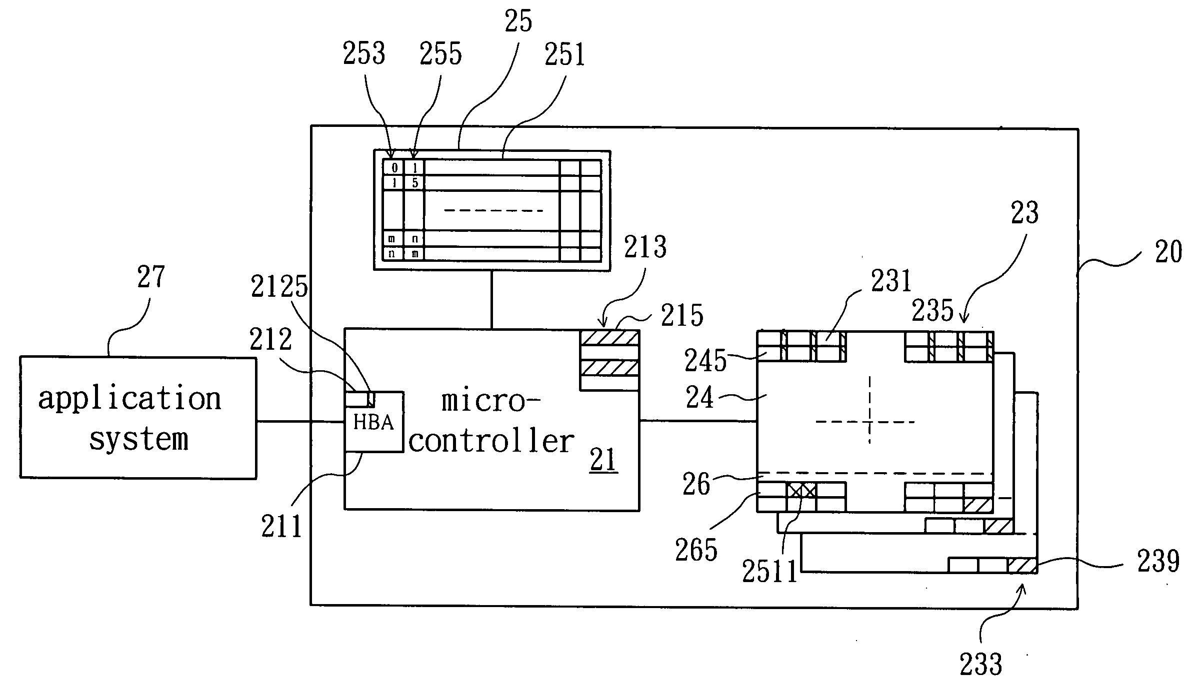
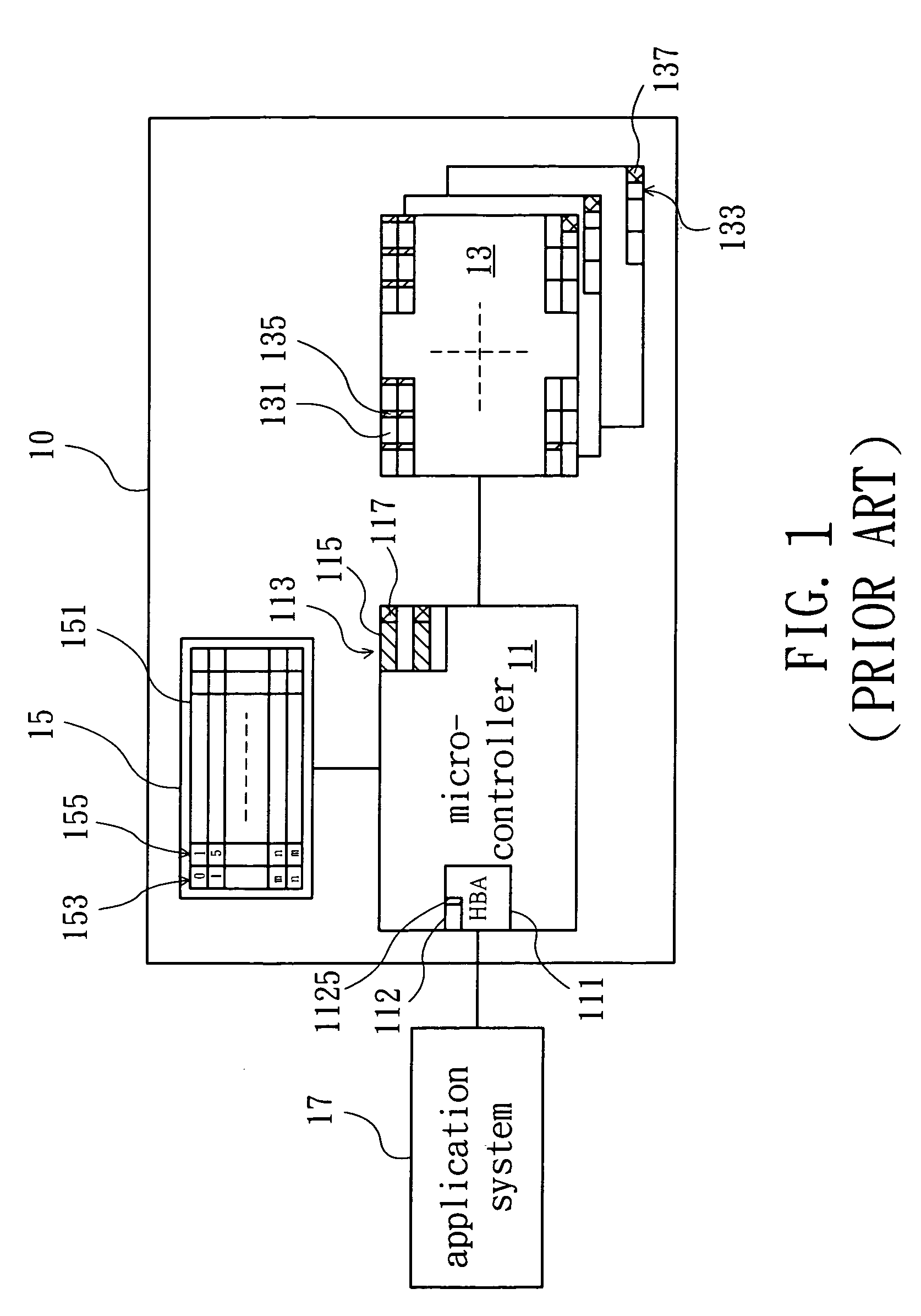
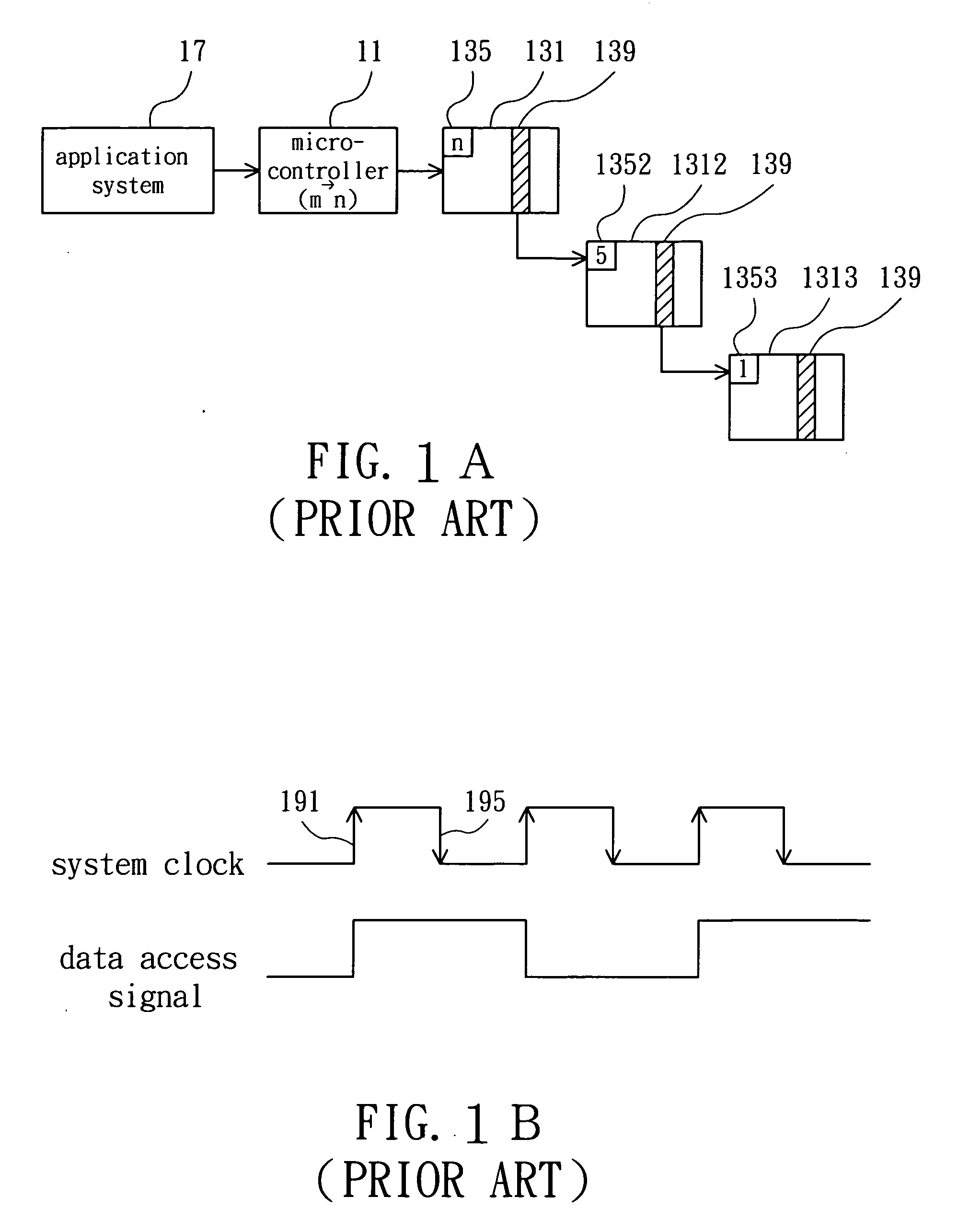
[0038] Firstly, referring to FIG. 2 collectively, there is shown a structural diagram of a flash storage according to one preferred embodiment of the present invention. As shown in this figure, a flash storage 20 of the present invention mainly comprises a micro-controller 21, a registered memory 25, and at least one flash memory (device) 23, in which the micro-controller 21 may be connected to the registered memory 25, the flash memory 23, and an application system 27, such as host system, player system, recording system, and so on. Moreover, the flash memory 23 further comprises a plurality of physical memory blocks 231, each having a physical address 235.

[0039] Generally, only reading or assigning a logical memory block 212 which, a plurality of logical memory blocks 212 bein...


PUM


Abstract

A flash storage comprises a flash memory, including a plurality of physical memory blocks, each of physical memory blocks comprising a plurality of memory segments, and a plurality of physical sectors, and each of physical sectors being further provided therein with at least a user data column and a logical address pointer column. When physical data is written into the user data column, writing logical address pointer data into the logical address pointer column of the same physical sector may be performed together by the control of a micro-controller. Furthermore, the logical address pointer data in the same memory segment are arranged to be a backup memory segment address mapping table and then stored in one physical memory block. The backup memory segment address mapping table may be loaded directly and stored into a registered memory by the micro-controller when the system boots. Thus, not only shortening the startup duration of the flash storage, but also saving the memory capacity of the registered memory and securing data access may be obtained.

Description

FIELD OF THE INVENTION [0001] The present invention relates to a flash storage allowed for not only shortening the startup duration thereof, but also saving the memory capacity of a registered memory and securing data access. BACKGROUND [0002] Accordingly, a conventional flash storage is shown in FIG. 1. A flash storage 10 mainly comprises a micro-controller 11, a registered memory 15, and at least one flash memory (device) 13, in which the micro-controller 11 may be connected to the registered memory 15, the flash memory 13, and a application system 17, while the flash memory 13 comprises therein a plurality of physical memory blocks 131, each of physical memories having one physical address 135. [0003] Generally, the application system 17 may be allowed to only read or assign a logical memory block 112 virtually presented in the micro-controller 11, a plurality of the logical memory blocks 112 being located in a logical memory block address (HBA) 111, according to the not exactly ...

Claims


Application Information

Patent Timeline
Patent Type & Authority Applications(United States)
IPC IPC(8): G06F12/00G06F12/16
CPCG06F12/0246
Inventor WANG, YU-HSIENLIN, CHANSONWU, TUNG-HSIENSU, CHIEN-CHANGLIN, GOW-JENGHSU, CHING-CHUNGCHEN, KUANG-YUAN
Owner PROLIFIC TECH INC
Why Eureka
Try Eureka