Defect image classifying method and apparatus and a semiconductor device manufacturing process based on the method and apparatus

a technology of defect image and manufacturing process, which is applied in the direction of image enhancement, semiconductor/solid-state device testing/measurement, instruments, etc., can solve the problems of consuming a greater amount of time and energy for operating personnel to analyze images, effectively presenting defect data to users for analysis, etc., to improve teaching efficiency and save user time and labor

Inactive Publication Date: 2006-12-07
HITACHI LTD
View PDF4 Cites 29 Cited by
  • Summary
  • Abstract
  • Description
  • Claims
  • Application Information

AI Technical Summary

Benefits of technology

[0012] An object of one embodiment of this invention is to provide a defect image classifying method and apparatus capable of improving the teaching efficiency in automatically classifying defect images according to teaching data given in advance, as well as a semiconductor device manufacturing process based on the method and apparatus; that is to provide, in an embodiment, a defect image classifying method and apparatus in which teaching data required to classify huge volumes of image data concerning contaminations or defects obtained from the particle inspection system or defect inspection system can be created while saving the user time and labor, and a semiconductor device manufacturing process based on the method and apparatus.

Problems solved by technology

However, as an increasing number of images are obtained, operating personnel must consume a greater amount of time and energy to analyze the images.
In addition, after teaching has occurred and automatic classification has been done, there still is the problem of effectively presenting the defect data to the user for analysis.

Method used


Image

  • Defect image classifying method and apparatus and a semiconductor device manufacturing process based on the method and apparatus
  • Defect image classifying method and apparatus and a semiconductor device manufacturing process based on the method and apparatus
  • Defect image classifying method and apparatus and a semiconductor device manufacturing process based on the method and apparatus

Examples


Embodiment Construction

[0038] Embodiments of this invention are described next referring to the attached drawings.

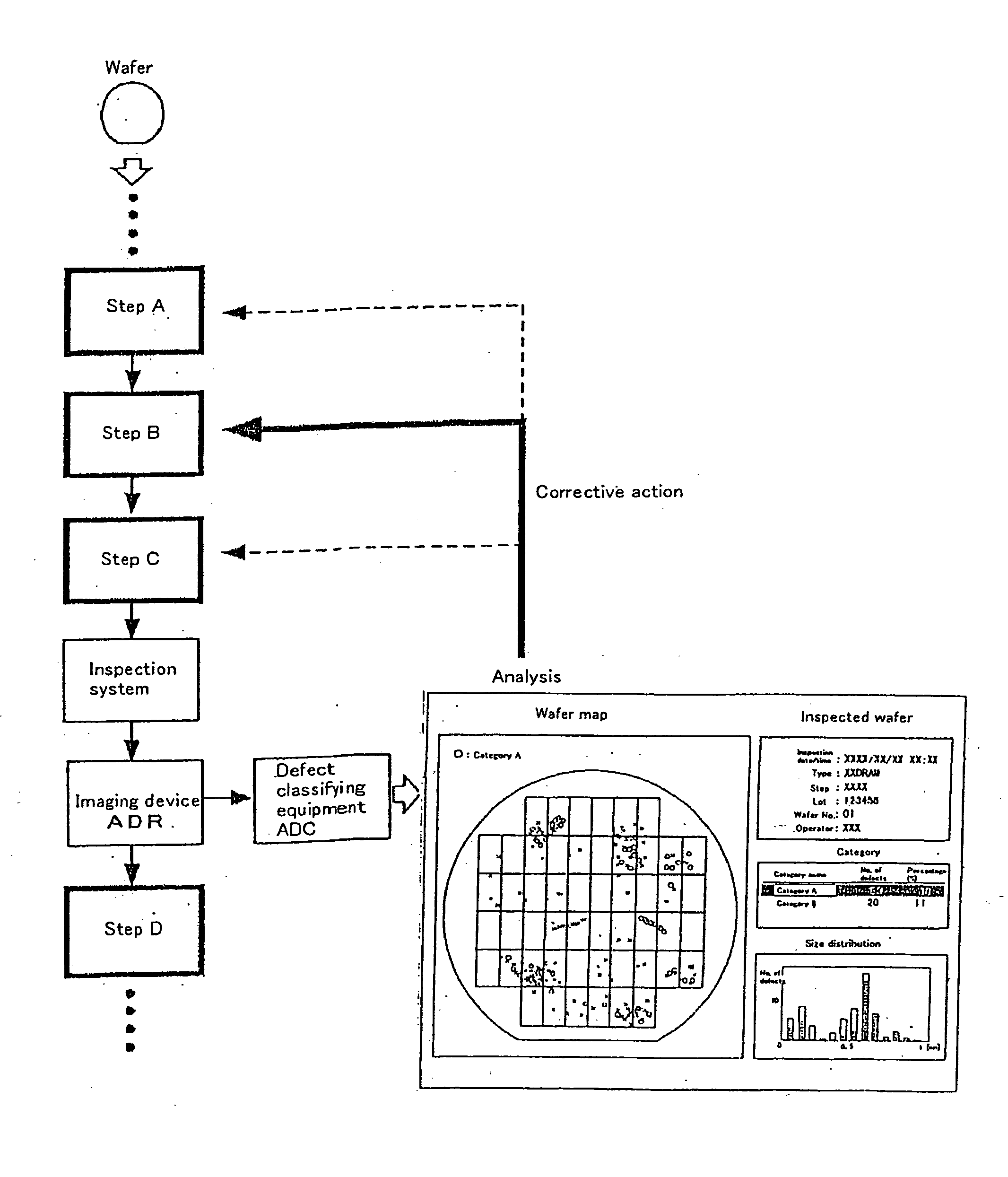
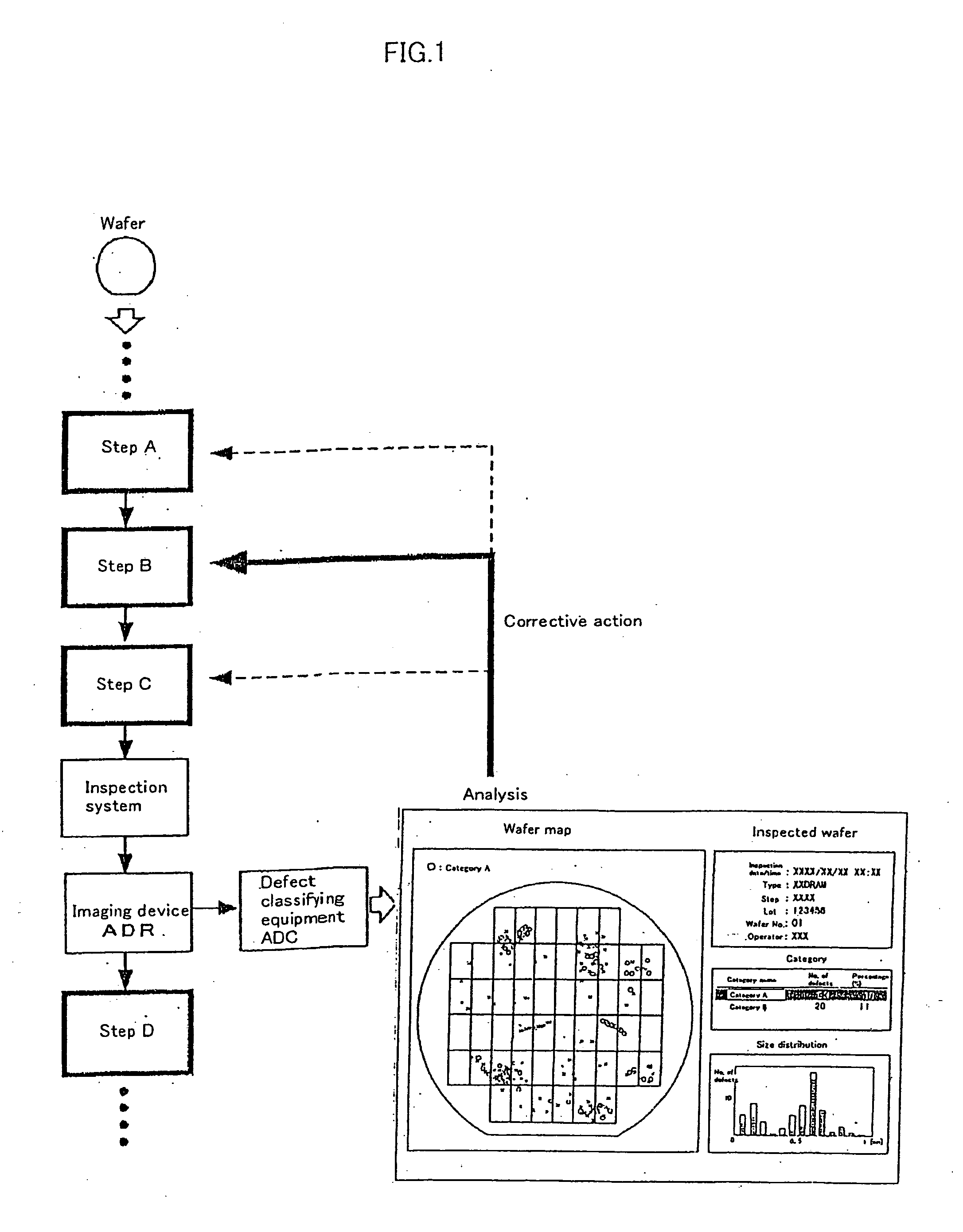
[0039]FIG. 1 shows the role of defect image classifying apparatus according to an embodiment of this invention, in the whole semiconductor manufacturing process. For a wafer which has undergone one or more processing steps, a contamination / defect inspection is made using a defect inspection system such as model I-890 from Hitachi, Ltd. and ADR is performed using an imaging device such as an SEM; the image data obtained by ADR is sent to defect classifying apparatus where ADC takes place to classify defect images into categories. Next for illustration purposes, it is assumed that a preliminary analysis has revealed that defects of categories A, B, and C frequently occur in step A, step B, and step C, respectively. A defect distribution by category, which gives the locations of defects of, for example, category B may be generated. If the defect distribution is abnormal, trouble in step B is sus...


PUM

PropertyMeasurementUnit
dAaaaaaaaaaa
dAaaaaaaaaaa
defect image classificationaaaaaaaaaa

Abstract

According to the present invention, techniques including a method and apparatus for classifying and displaying images are provided. In an embodiment of the present invention a defect image classification method using inspected objects is provided. The method includes defect images obtained from at least one inspected object. Next a set of defect images is classified into a specified category, which has a feature. The defect images are arranged for display according to the feature and then displayed. The arranging of the defect images may also be based on an evaluation value for each defect image. Another embodiment provides a defect image classification method using inspected objects. Defect images are obtained from at least one inspected object. Next the defect images are classified into a plurality of categories and at least two information items for example, a defect distribution diagram showing locations of defects in the inspected object, information associated with a category of the plurality of categories, and a defect size distribution, are displayed.

Description

CROSS-REFERENCES TO RELATED APPLICATIONS [0001] This application is a Continuation Application of U.S. patent application Ser. No. 09 / 716,077, filed Nov. 17, 2000, which is related to and claims priority from Japanese Patent Application No. 11-337196 filed on Nov. 29, 1999, both of which are incorporated by reference herein in their entirety for all purposes. [0002] This application is related to the following commonly assigned, non-provisional patent application, the disclosure of which is herein incorporated by reference in its entirety: [0003] U.S. patent application Ser. No. 09 / 661,182 filed Sep. 13, 2000.BACKGROUND OF THE INVENTION [0004] This invention relates to a method and apparatus for classifying defect images obtained by imaging of contaminations or defects detected on semiconductor wafers and a semiconductor device manufacturing process based on the method and apparatus. [0005] A semiconductor device is manufactured by making a wafer as a substrate go through several pr...

Claims


Application Information

Patent Timeline
Patent Type & Authority Applications(United States)
IPC IPC(8): G06K9/00G06K9/62G01N21/88G06T7/00H01L21/66
CPCG06T2207/30148G06T7/001
Inventor OBARA, KENJITAKAGI, YUJINAKAGAKI, RYOOZAWA, YASUHIROKUROSAKI, TOSHIEIISOGAI, SEIJI
Owner HITACHI LTD
Why Eureka
Try Eureka