Apparatus and methods for packaging antennas with integrated circuit chips for millimeter wave applications

a technology of integrated circuit chips and antennas, applied in the direction of antennas, antenna details, semiconductor devices, etc., can solve the problems of high cost and bulky, and achieve the effect of increasing the dimension of radio communication systems and highly integrated radio/wireless communication systems

Inactive Publication Date: 2006-12-07
IBM CORP
View PDF28 Cites 110 Cited by
  • Summary
  • Abstract
  • Description
  • Claims
  • Application Information

AI Technical Summary

Benefits of technology

The patent describes how technology advancements have made it possible to integrate antennas into tiny electronics packages that also contain other components like microprocessors or memory. This allows for more efficient use of space when designing wireless communication systems for things like phones or computers. The method involves constructing the antennas within the framework of the package structure itself.

Problems solved by technology

The technical problem addressed by this patent is how to create efficient and effective wireless communication networks where different devices can easily communicate wirelessly without being limited by individual component mounting levels and high costs associated with traditional methods.

Method used


Image

  • Apparatus and methods for packaging antennas with integrated circuit chips for millimeter wave applications
  • Apparatus and methods for packaging antennas with integrated circuit chips for millimeter wave applications
  • Apparatus and methods for packaging antennas with integrated circuit chips for millimeter wave applications

Examples


Embodiment Construction

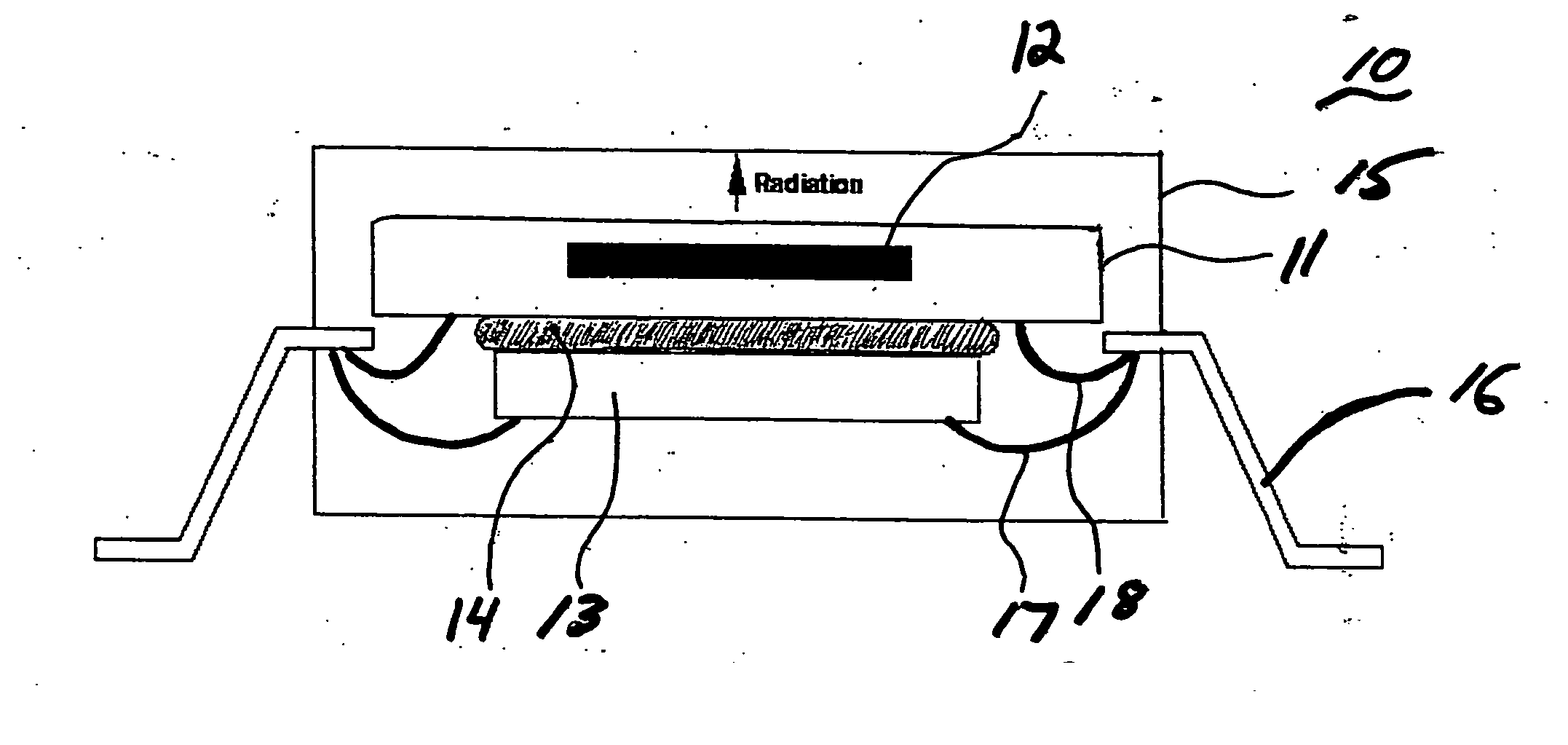
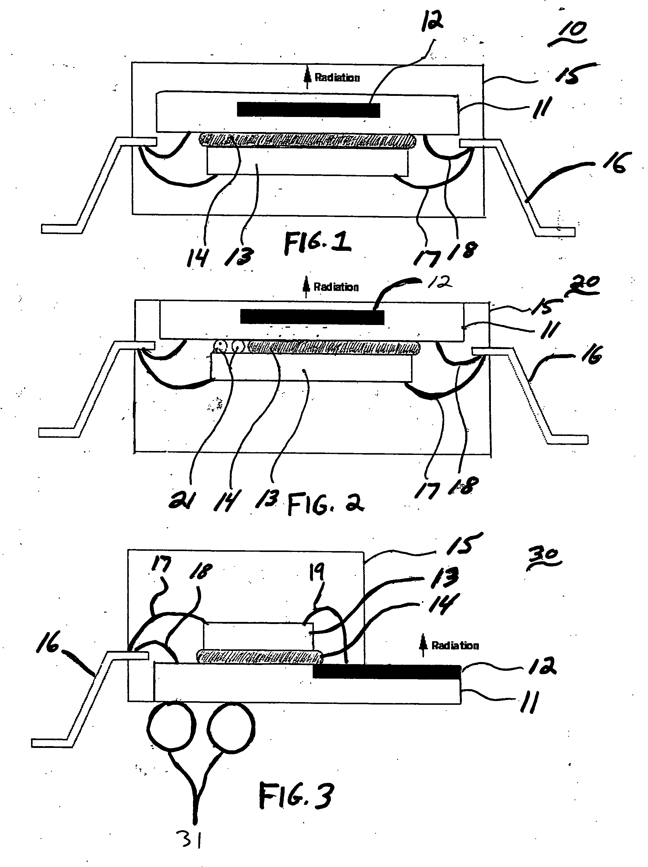
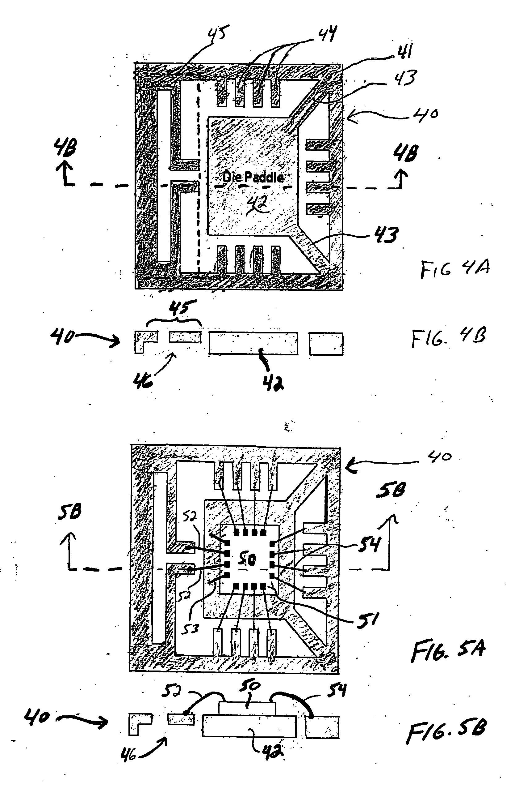
[0024] Exemplary embodiments of the invention as described in detail hereafter generally include apparatus and methods for integrally packaging antenna devices and semiconductor IC chips to form electronic devices having highly-integrated, compact radio / wireless communications systems for millimeter wave applications. More specifically, exemplary embodiments of the invention include apparatus and methods for integrally packaging IC chips with antenna devices having radiating elements that are integrally constructed from one of various types of package frame structures that are commonly used for constructing chip packages. In general, package frames are those structures commonly used for constructing chip packages, which function to, e.g., provide mechanical stability to the chip package, provide chip bond sites for mechanically mounting one or more IC chips (or dies), and provide electrical lines and / or contacts that are used for making electrical connections to the IC chip(s) mount...


PUM


Abstract

Apparatus and methods are provided for integrally packaging semiconductor IC (integrated circuit) chips and antenna devices which are integrally constructed from package frame structures (e.g., lead frame, package carrier, package core, etc.), to thereby form compact integrated radio/wireless communications systems for millimeter wave applications.

Description


Claims


Application Information

Patent Timeline
Owner IBM CORP
Why Eureka
Try Eureka