Organic EL device

a technology of organic el and device, which is applied in the direction of organic semiconductor devices, discharge tube luminescnet screens, natural mineral layered products, etc., can solve the problems of high operating voltage of organic el devices, difficult to find holes, and the operation of top-emission-type organic el devices may not be easy

Active Publication Date: 2006-12-14
UDC IRELAND
View PDF3 Cites 57 Cited by
  • Summary
  • Abstract
  • Description
  • Claims
  • Application Information

AI Technical Summary

Problems solved by technology

However, the electron hole may not be easily injected directly from the Ag or Al layer into the organic layer 13, causing a rise in operating voltage of the organic EL device.
However, according to the present inventor's findings, the top-emission-type organic EL device still has technical problems associated with the operation life, and no case of realization of a lifetime long enough to endure practical use has been reported.
In particular, a device comprising an Al / Ni anode disclosed in the above-mentioned J. Appl. Phys., Vol. 94, No. 8, 5290 (2003), for example, exhibits inferior life property.

Method used


Image

  • Organic EL device
  • Organic EL device
  • Organic EL device

Examples


example 1

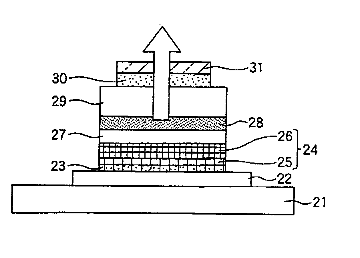
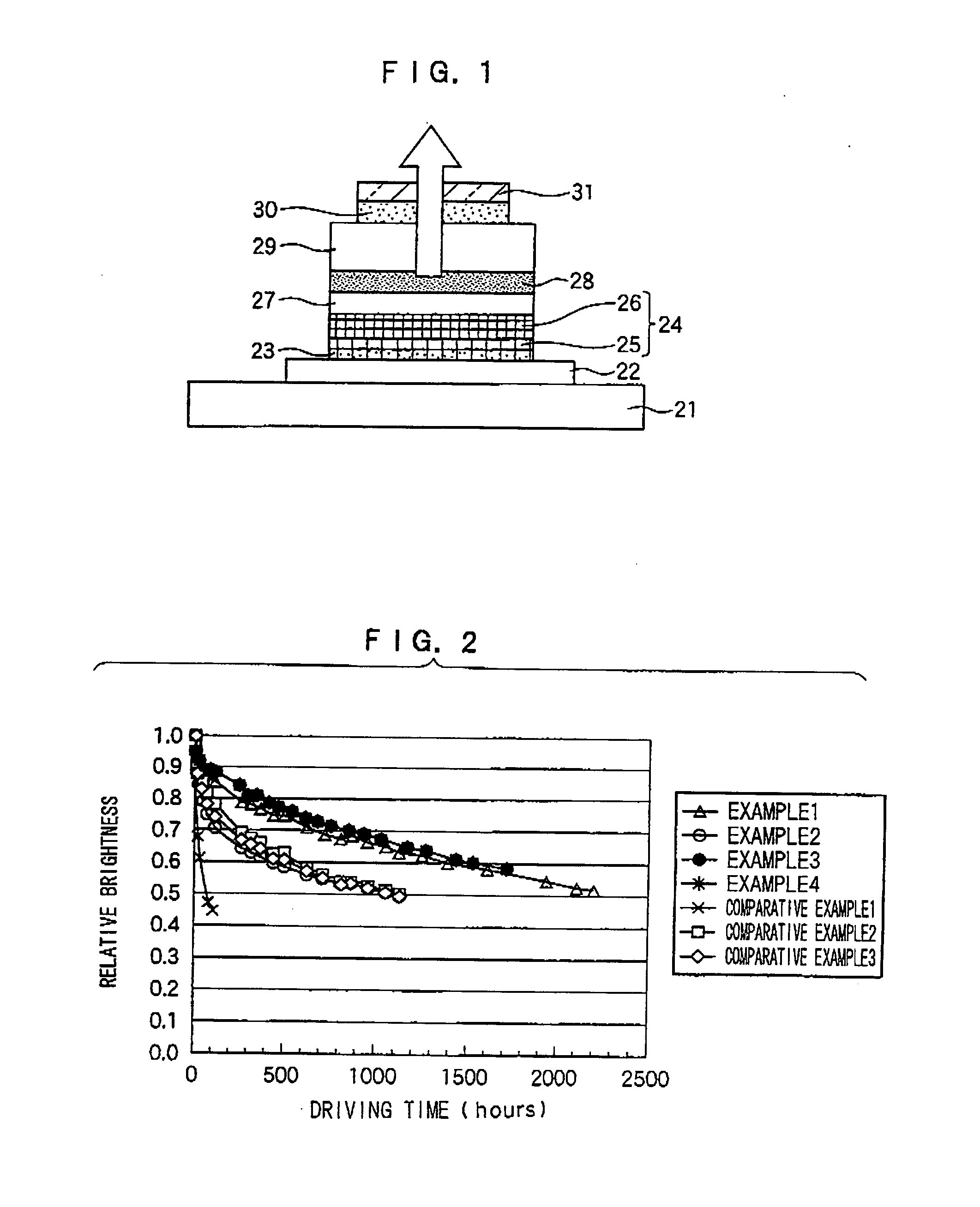
[0067] (1) A glass substrate is subjected to an ultrasonic-wave cleaning with pure water, an acetone, pure water, and an IPA in the order thereof, for 15 minutes respectively.

[0068] (2) A light-reflective anode having a thickness of 60 nm is formed by performing a vapor deposition using a W filament to form an Al layer, and thereafter the surface of the substrate is treated with UV ozone for 20 minutes.

[0069] (3) A first hole-injection layer having a thickness of 20 nm is formed by performing a codeposition in accordance with a vacuum-deposition method, wherein a Ta boat and a Mo boat are used for a 2-TNATA and a V2O5 respectively so that the doping density of V2O5 is 33% by weight.

[0070] (4) A second hole-injection layer having a thickness of 165 nm is formed by performing a codeposition in accordance with a vacuum-deposition method, wherein a Ta boat and also a Ta boat are used for a 2-TNATA and a F4-TCNQ respectively so that the doping density of F4-TCNQ is 0.1% by weight.

[00...

example 2

[0078] In EXAMPLE 2, a Ni anode buffer layer having a thickness of 1 nm is formed on the Al light-reflective anode by performing a vapor deposition in accordance with a vacuum-deposition method, using a W filament, before the surface of the substrate is treated with a UV ozone for 20 minutes.

[0079] Accordingly, the hole-injection layer of EXAMPLE 2 is formed on the Ni layer, not on the Al layer as in the case of EXAMPLE 1.

example 3

[0080] In EXAMPLE 3, a MoO3 anode buffer layer having a thickness of 2 nm is formed on the Al light-reflective anode by performing a vapor deposition in accordance with a vacuum-deposition method, using a Mo boat.

[0081] Accordingly, the hole-injection layer of EXAMPLE 3 is formed on the MoO layer, not on the Al or the Ni layer as in the case of EXAMPLE 1 or EXAMPLE 2.

[0082] Additionally, the thickness of the second bole-injection layer in EXAMPLE 3 is 170 nm, not 165 nm as in the case of EXAMPLE 2.


PUM

PropertyMeasurementUnit
work functionaaaaaaaaaa
thicknessaaaaaaaaaa
thicknessaaaaaaaaaa

Abstract

A top-emission-type organic EL device comprising a substrate and at least a light-reflective anode, a bole-injection layer comprising first and second hole-injection layers, a hole-transport layer, a light-emitting layer, an electron-transport layer, and a light-transmitting cathode, which are sequentially laminated on the substrate, wherein the light-reflective anode side of hole-injection layer (the first hole-injection layer) is doped with a metallic oxide.

Description

CROSS-REFERENCE TO RELATED APPLICATION [0001] This application claims priority under 35 USC 119 from Japanese Patent Application No. 2005-154951, the disclosure of which is incorporated by reference herein. BACKGROUND OF THE INVENTION [0002] 1. Field of the Invention [0003] The present invention relates to a method to achieve higher light-emission efficiency and longer operating life for a top-emission-type organic EL device, in which light is taken out from the upper electrode of the device. [0004] 2. Description of the Related Art [0005] A display apparatus in which an organic EL device can be practically used as a display device is currently under active research and development. [0006] Particularly, a top-emission-type organic EL device, in which light is emitted through an upper electrode provided on the opposite side of a substrate, has an advantage over a bottom-emission-type organic EL device, in which light is emitted through a lower electrode on the side of a substrate, es...

Claims


Application Information

Patent Timeline
Patent Type & Authority Applications(United States)
IPC IPC(8): H01L51/50H05B33/12
CPCB82Y20/00B82Y30/00H01L2251/5369H01L51/5271H01L2251/5315H01L51/5206H10K50/17H10K50/818H10K50/828H10K50/856H10K2102/331H10K2102/3026
Inventor NAKAYAMA, MASAYA
Owner UDC IRELAND
Why Eureka
Try Eureka