Organic light emitting diode device and method of manufacturing the same

a light-emitting diode and organic technology, applied in the direction of discharge tube luminescnet screens, discharge tube/lamp details, electric discharge lamps, etc., can solve the problems of failure of light emission, corresponding deterioration of display quality, and failure of emission layer to cover the entire surface of the injection layer, so as to prevent loss and damage of the injection layer

Inactive Publication Date: 2009-06-18
SAMSUNG ELECTRONICS CO LTD
View PDF3 Cites 46 Cited by
  • Summary
  • Abstract
  • Description
  • Claims
  • Application Information

AI Technical Summary

Benefits of technology

[0009]In accordance with one or more embodiments of the present invention, an organic light-emitting diode device is disclosed that can prevent the direct contact of the hole injection layer and the cathode electrode and acquire even display properties, and can prevent the loss and damage of the hole injection layer during the formation of the barrier rib by forming an inorganic insulating layer on the hole injection layer before the formation of the barrier rib.

Problems solved by technology

An interfacial phenomenon occurs when the hole injection layer is formed between the barrier ribs and may cause the hole injection layer to be uneven, so that an emission layer may fail to cover the entire surface of the hole injection layer.
This may result in a direct contact between a cathode electrode and the hole injection layer which may cause a failure of light emission and corresponding deterioration in display quality.

Method used


Image

  • Organic light emitting diode device and method of manufacturing the same
  • Organic light emitting diode device and method of manufacturing the same
  • Organic light emitting diode device and method of manufacturing the same

Examples


Embodiment Construction

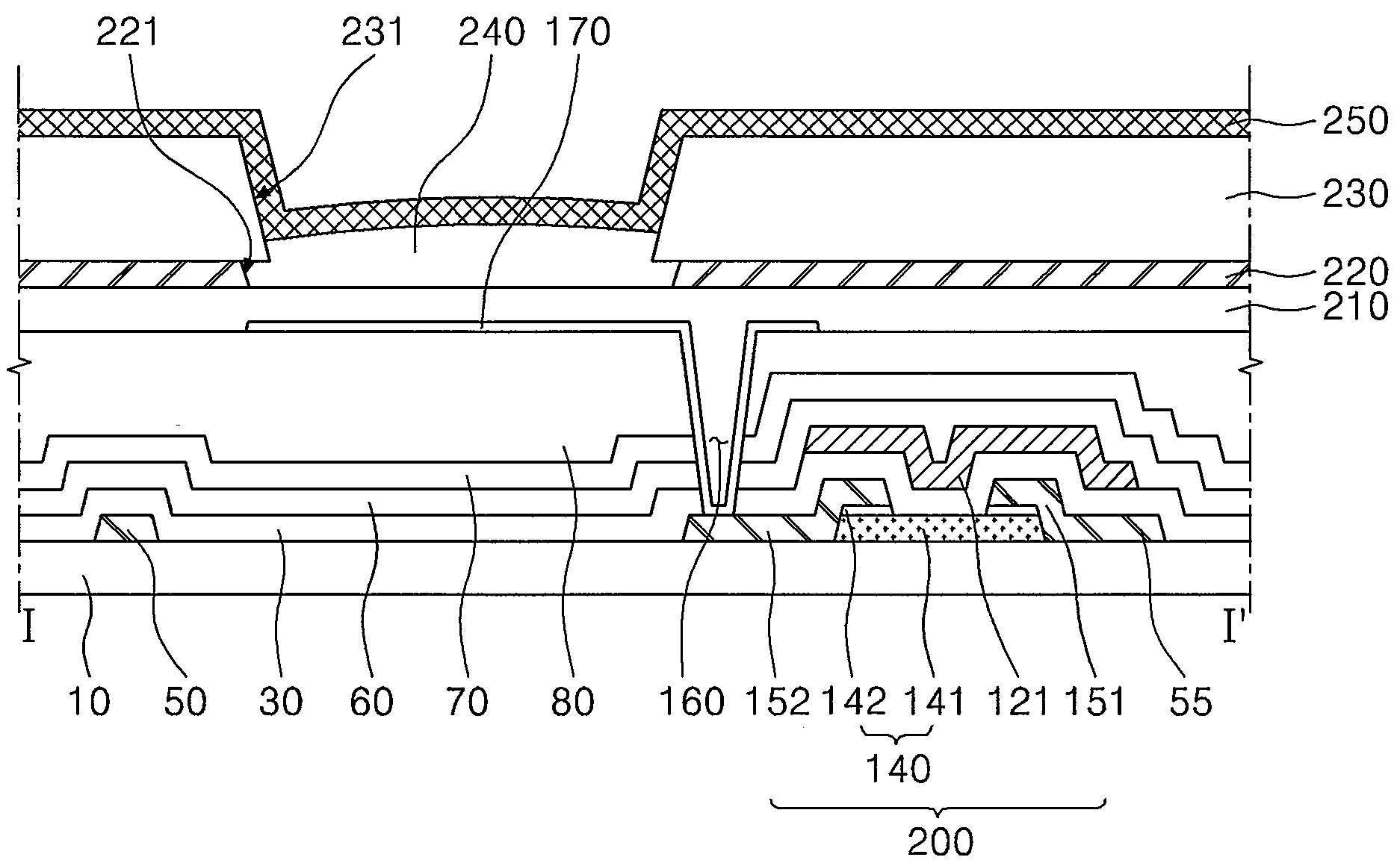
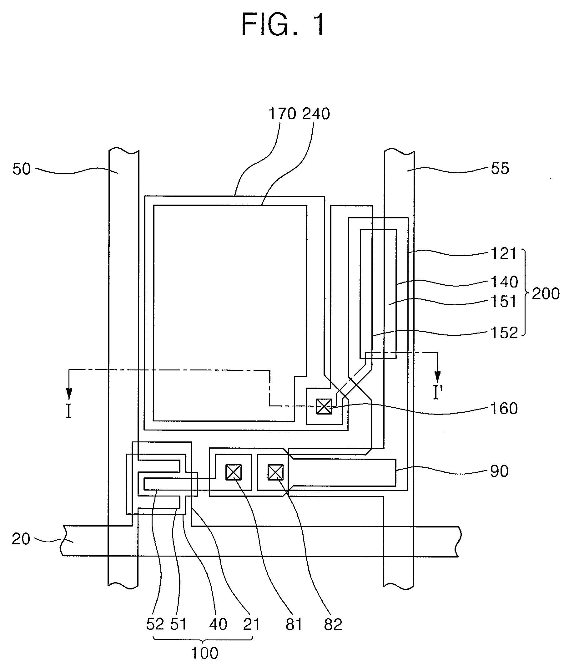
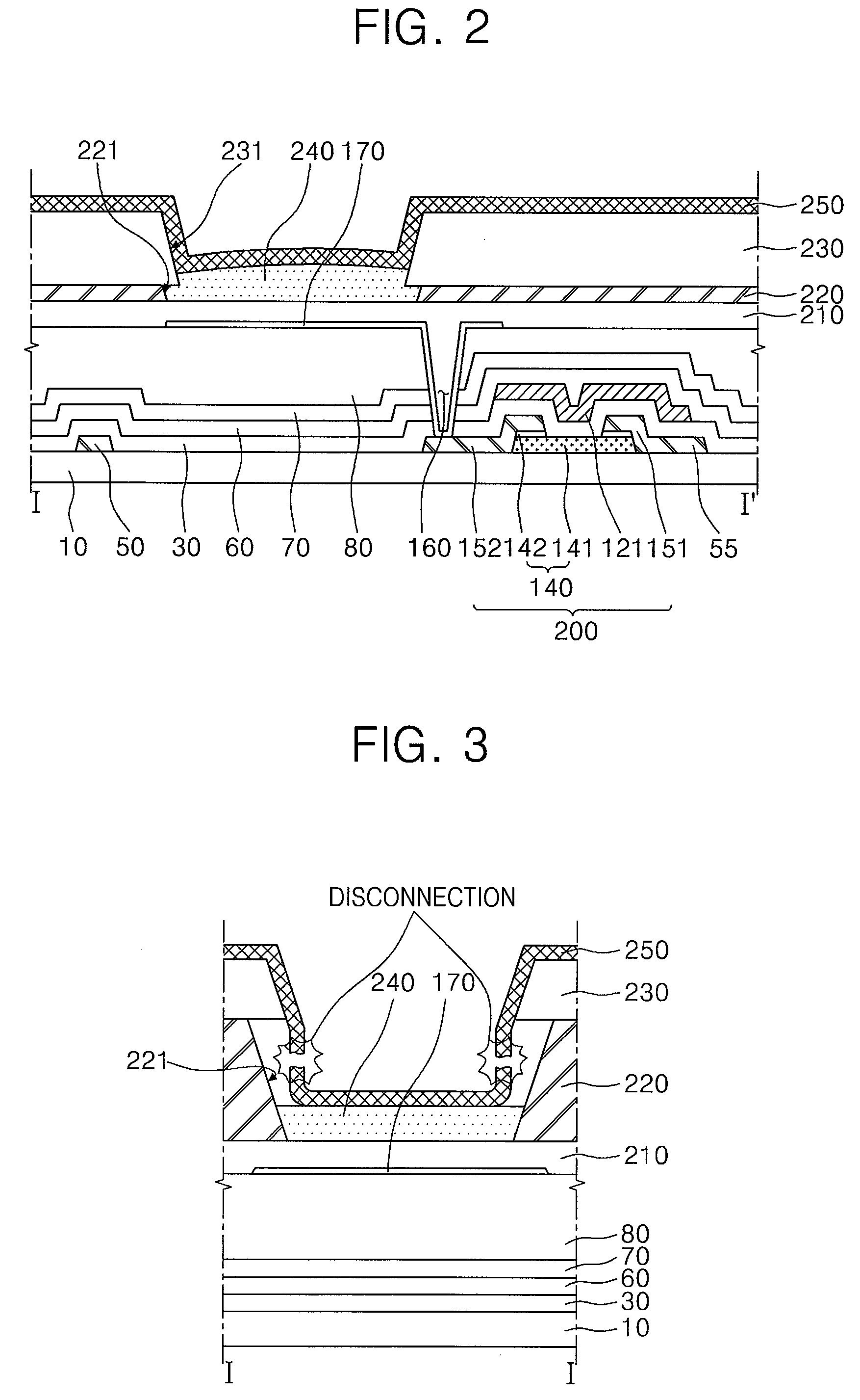
[0036]Embodiments of the invention will be described more fully hereinafter with reference to the accompanying drawings, in which various embodiments of the invention are shown. This invention may, however, be embodied in many different forms and should not be construed as limited to the embodiments set forth herein. Rather, these embodiments are provided so that this disclosure will be thorough and complete, and will fully convey the scope of the invention to those skilled in the art. Like reference numerals refer to like elements throughout.

[0037]It will be understood that when an element is referred to as being “on” another element, it can be directly on the other element or intervening elements may be present there between. In contrast, when an element is referred to as being “directly on” another element, there are no intervening elements present. As used herein, the term “and / or” includes any and all combinations of one or more of the associated listed items.

[0038]It will be u...


PUM


Abstract

An organic light-emitting diode device and a method of manufacturing the organic light-emitting diode device are disclosed. The organic light-emitting diode device includes a thin film transistor, an anode electrode electrically connected to the thin film transistor, a hole injection layer formed on the anode electrode, an etch-out buffer layer formed on the hole injection layer, the etch-out buffer layer having a first hole that exposes the hole injection layer, a barrier rib formed on the etch-out buffer layer, the barrier rib having a second hole that overlaps the first hole, an organic emission layer formed on a portion of the hole injection layer which is exposed through the first hole and second hole, and a cathode electrode formed on the organic emission layer.

Description

CROSS-REFERENCE TO RELATED APPLICATION[0001]This application claims priority to and the benefit of Korean Patent Application No. 10-2007-0129188, filed in the Korean Intellectual Property Office on Dec. 12, 2007, the disclosure of which is incorporated herein by reference in its entirety.BACKGROUND[0002]1. Technical Field[0003]The present invention generally relates to an organic light-emitting diode device whose organic light emitting layer is evenly formed and a method of manufacturing the organic light-emitting diode device.[0004]2. Description of the Related Art[0005]Generally, organic light-emitting diode (OLED) devices are next generation display devices that have high energy efficiency with reduced power consumption.[0006]OLED devices include a substrate, thin film transistors (TFTs) formed on the substrate, and OLEDs electrically connected to the TFTs. At least one TFT is provided near each pixel to drive the OLED.[0007]The OLED includes an anode electrode, a cathode electro...

Claims


Application Information

Patent Timeline
Patent Type & Authority Applications(United States)
IPC IPC(8): H01L51/10H01L51/40
CPCH01L27/3246H01L51/56H01L51/0012H10K59/122H10K71/191H10K71/00H05B33/22
Inventor LEE, DONG-WONCHU, CHANG-WOONGCHUNG, JIN-KOO
Owner SAMSUNG ELECTRONICS CO LTD
Why Eureka
Try Eureka