White organic light emitting device

a light-emitting device and organic technology, applied in the direction of thermoelectric device junction materials, semiconductor devices, electrical equipment, etc., can solve the problems of large-sized shadow masks that can be sagging, and achieve the effects of enhancing panel efficiency and color reproduction range, reducing power consumption, and easy injection of holes

Active Publication Date: 2014-06-19
LG DISPLAY CO LTD
View PDF2 Cites 45 Cited by
  • Summary
  • Abstract
  • Description
  • Claims
  • Application Information

AI Technical Summary

Benefits of technology

[0015]Also, the embodiments are to provide a white organic light emitting device which is easy to inject holes by enabling a host of a light emission layer of a second stack adjacent to a hole transportation layer to be formed the same material as the hole transportation layer.
[0016]Moreover, the embodiments are to provide a white organic light emitting device that is adapted to enhance panel efficiency and color reprod

Problems solved by technology

However, a large-sized shadow mask can be sagged due to its load (or its weight).
However, it is necessary (or difficult) for the white OLED dev

Method used


Image

  • White organic light emitting device
  • White organic light emitting device
  • White organic light emitting device

Examples


first embodiment

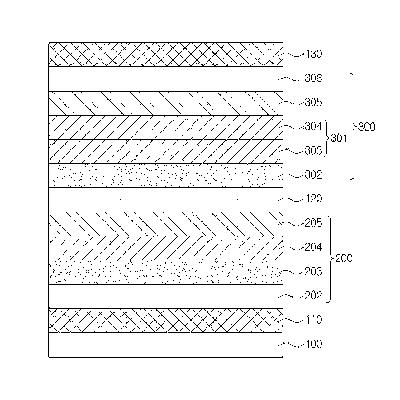
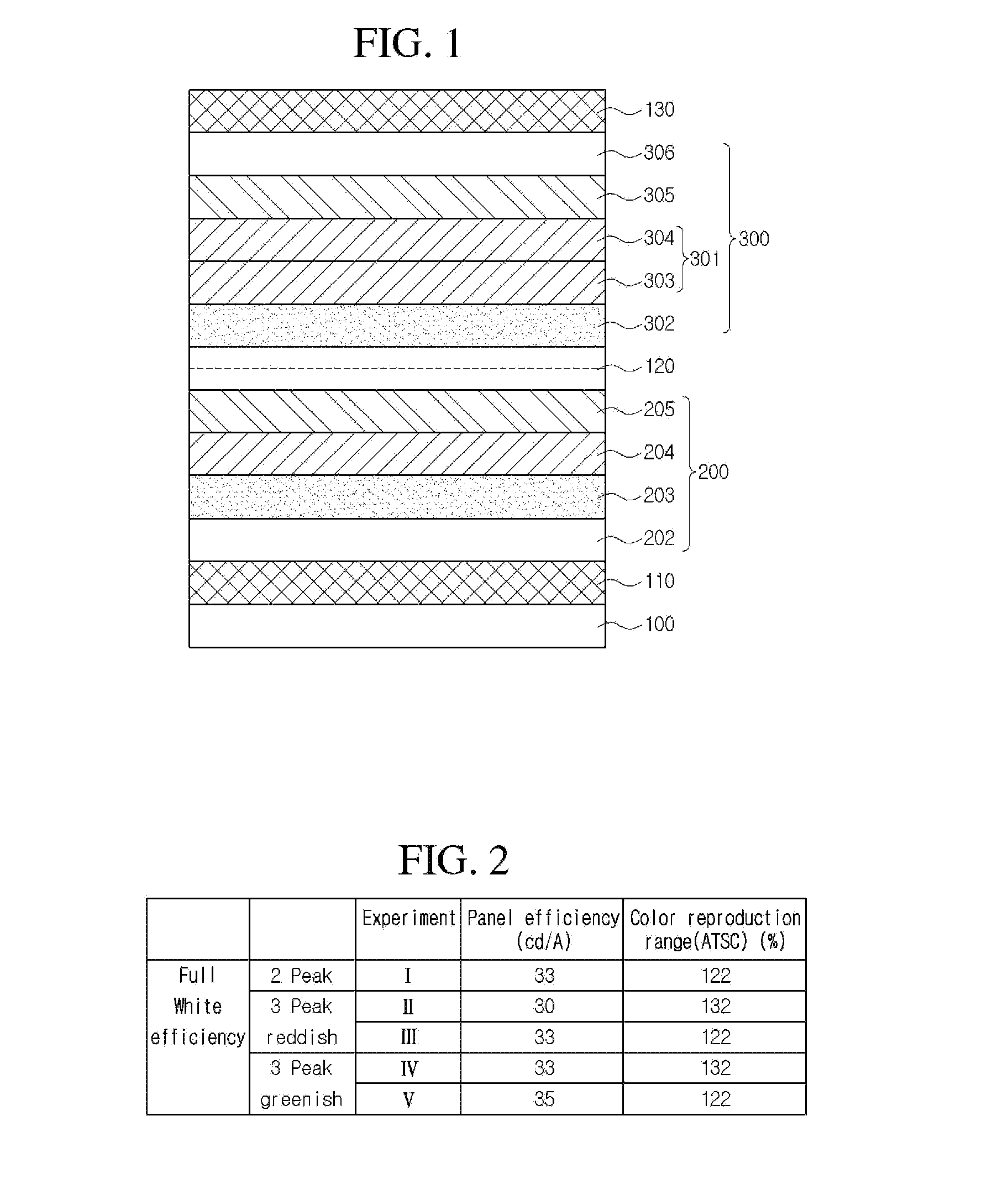
[0033]FIG. 1 is a cross-sectional view showing a white organic light emitting device according to the present disclosure.

[0034]Referring to FIG. 1, the white organic light emitting device according to a first embodiment of the present disclosure includes first and second electrodes 110 and 130 formed on a substrate 100 in such manner as to face each other. A first stack 200, a charge generation layer 120 and a second stack 300 are interposed between the first and second electrodes 110 and 130. The first stack 200, the charge generation layer 120 and the second stack 300 can be formed by being sequentially stacked on the first electrode 110. The first and second stacks 200 and 300 include different color light emission layers from each other. Different color lights emitted from the light emission layers of the first and second stacks 200 and 300 are mixed, thereby realizing white light.

[0035]The substrate 100 can become an insulation substrate. A thin film transistor (not shown) can ...

second embodiment

[0070]FIG. 7 is a cross-sectional view showing a white organic light emitting device according to the present disclosure.

[0071]Referring to FIG. 7, the white organic light emitting device according to a second embodiment of the present disclosure includes first and second electrodes 110 and 130 formed on a substrate 100 in such manner as to face each other. A first stack 400, a first charge generation layer 220, a second stack 500, a second charge generation layer 320 and a third stack 600 are interposed between the first and second electrodes 110 and 130. The first stack 400, the first charge generation layer 220, the second stack 500, the second charge generation layer 320 and the third stack 600 can be formed by being sequentially stacked on the first electrode 110.

[0072]The first through third stacks 400, 500 and 600 can include the same color light emission layer. Alternatively, the second stack 500 can include a different color light emission layer from those of the first and ...


PUM


Abstract

A white organic light emitting device includes: first and second electrodes formed to face each other on a substrate; a first stack configured with a hole injection layer, a first hole transportation layer, a first light emission layer and a first electron transportation layer which are stacked between the first and second electrodes; a second stack configured with a second hole transportation layer, a second light emission layer, a third light emission layer, a second electron transportation layer and an electron injection layer which are stacked between the first stack and the second electrode; and a charge generation layer interposed between the first and second stacks and configured to adjust a charge balance between the two stacks.

Description

[0001]The present application claims priority under 35 U.S.C. §119(a) of Korean Patent Application No. 10-2012-0148300 filed on Dec. 18, 2012 and Korean Patent Application No. 10-2013-0114553 filed on Sep. 26, 2013, which are hereby incorporated by references in their entireties.BACKGROUND[0002]1. Field of the Disclosure[0003]The present application relates to an organic light emitting device, and more particularly to a white organic light emitting device adapted to enhance efficiency and color reproduction range and reduce power consumption.[0004]2. Description of the Related Art[0005]Nowadays, a display field for visually representing an electrical information signal has been rapidly developed with the spread of substantial information society. In accordance therewith, a variety of flat panel display devices with features, such as slimness, light weight and low power consumption have been developed. Also, the flat panel display devices have been rapidly replacing the existing cath...

Claims


Application Information

Patent Timeline
IPC IPC(8): H01L51/52
CPCH01L51/5262H10K50/131H10K50/11H10K2101/10H10K59/32H10K50/13H10K2101/27H10K2101/90H10K2102/351H10K50/125H10K50/19H10K50/121H10K50/15H10K50/16H10K50/17H10K50/81H10K50/82H10K50/171
Inventor YOO, TAE SUNKIM, HWA KYUNGCHOI, HONG SEOKSONG, JAE ILHAN, MI YOUNGKIM, SHIN HANOH, HYE MIN
Owner LG DISPLAY CO LTD
Why Eureka
Try Eureka