Charge injection and transport layers

a technology of charge injection and transport layer, which is applied in the direction of sustainable manufacturing/processing, non-metal conductor manufacturing, and final product manufacturing, etc., can solve the problems of difficult problems of hole injection layer and hole transport layer, and achieve the effects of improving the efficiency of organic electronic device, improving device life, and increasing device efficiency

Active Publication Date: 2010-05-06
NISSAN CHEM IND LTD
View PDF4 Cites 49 Cited by
  • Summary
  • Abstract
  • Description
  • Claims
  • Application Information

AI Technical Summary

Benefits of technology

[0005]The compositions can comprise at least one conductive conjugated polymer, at least one semiconducting matrix component that is different from the conductive conjugated polymer, and an optional dopant, and can be substantially free of an insulating matrix component. The compositions can produce improved HILs and HTLs that, when incorporated into electronic devices such as OLEDs or OPVs, can lead to increases in the performance of the devices.
[0010]In yet other aspects, a method is provided for improving the efficiency of an organic electronic device, the method comprising: providing a hole transport layer or hole injection layer comprising (a) at least one conductive conjugated polymer, (b) at least one semiconducting matrix component that is different from the conductive conjugated polymer in (a), and (c) optionally, at least one dopant, wherein the hole transport layer or hole injection layer is substantially free of an insulating matrix component; and incorporating the hole transport layer or hole injection layer into the organic electronic device; wherein incorporation of the hole transport layer or hole injection layer into the organic electronic device leads to an increase in device efficiency of at least 5%.
[0011]At least one advantage for at least one embodiment is improved device lifetime.
[0012]At least one advantage for at least one embodiment is improved combinations of device properties, including device performance and / or device lifetime.
[0013]At least one additional advantage for at least one embodiment is improved formulation flexibility.

Problems solved by technology

Hole injection layers and hole transport layers can present difficult problems because of the solubilities of the component materials (or lack their of) in processing solvents, and because of the dopants and / or acids needed for HIL or HTL performance.

Method used


Image

  • Charge injection and transport layers
  • Charge injection and transport layers
  • Charge injection and transport layers

Examples


working examples

Example 1

Representative Formulations

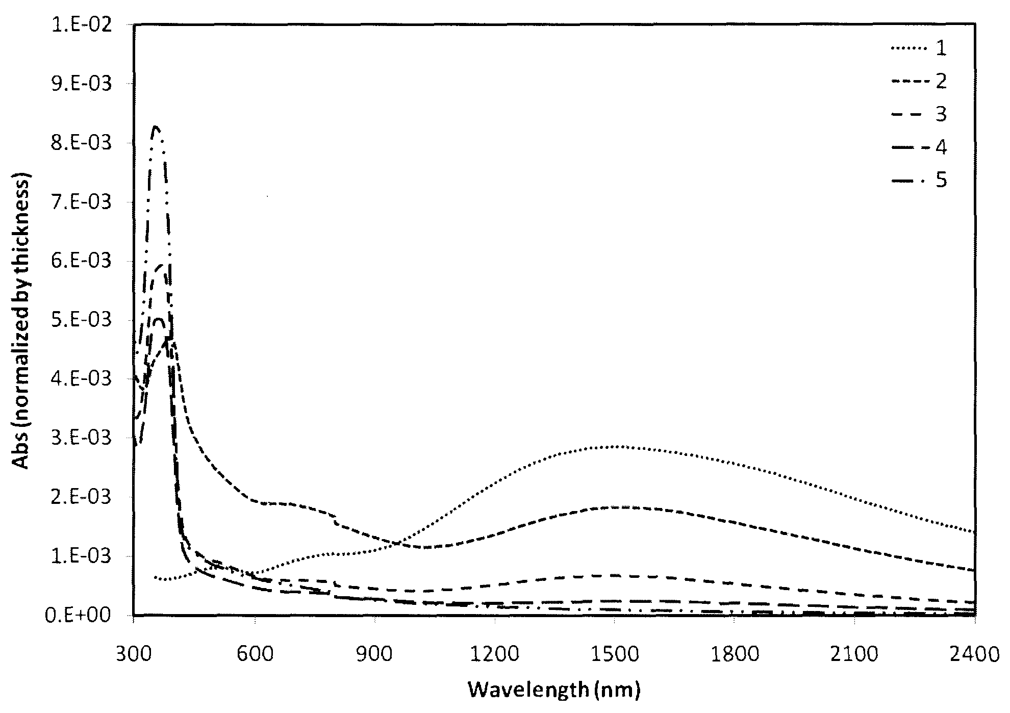
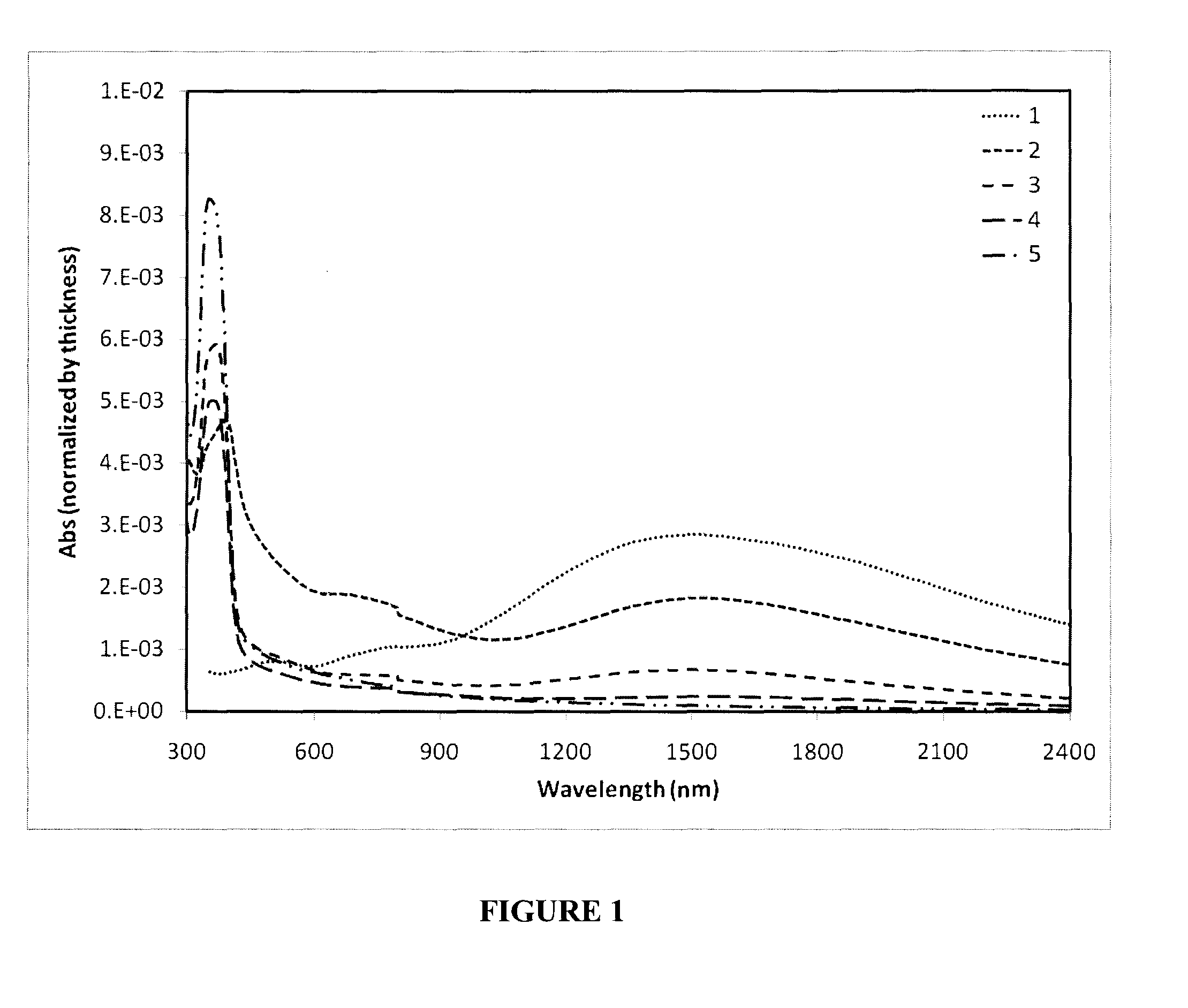
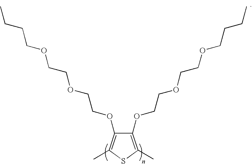
[0118]A series of HIL ink formulations were prepared containing PDBEETh and IMDPIB(PhF5)4 as conductive conjugated polymer and dopant, and NPB as semiconducting matrix polymer, as shown in Table 1 below.

[0119]The ink formulations were obtained using the following general procedure: Separate stock solutions of PDBEETh and IMDPIB(PhF5)4 in CHCl3 were first prepared, each containing 0.5% (w / w) solids. Various amounts of each stock solution were combined as indicated in Table 1. For each formulation, the stock solution of IMDPIB(PhF5)4 was added to the PDBEETh stock solution so that the moles of IMDPIB(PhF5)4 dopant per repeat unit of the PDBEETh polymer was kept at 0.3. The resulting combined solution was refluxed for 2 h under a nitrogen blanket and stored in the glove-box. The indicated weight percent of NPB (added as a 0.5% (w / w) stock solution in chloroform) was added to the doped PDBEETh to prepare the final ink formulation.

TABLE 1Composition of...

example 2

OLED Device Fabrication

[0122]OLED devices were fabricated following procedures known in the art. The devices were fabricated on indium tin oxide (ITO) surfaces deposited on glass substrates. The ITO surface was pre-patterned to define the pixel area of 0.05 cm2. The device substrates were cleaned by ultrasonication in a dilute soap solution for 20 minutes followed by distilled water washes. This was followed by ultrasonication in isopropanol for 20 minutes. The substrates were dried under nitrogen flow, followed by treatment in a UV-Ozone chamber operating at 300 W for 20 minutes.

[0123]The cleaned substrates were then coated with an HIL ink formulation and dried at 90-170° C. for 5-15 minutes to form an HIL film layer. Dry film thicknesses ranged from approximately 20 nm to 60 nm. The coating process was done on a spin coater, but can be similarly achieved with spray coating, ink-jetting, contact printing, or any other deposition method capable of resulting in an HIL film of the des...

example 3

OLED Device Testing

[0127]Performance tests were conducted on the OLED devices of Example 2. Typically, performance is quantified by a combination of different parameters such as operating voltage (should be low), brightness in nits (should be bright, luminous), efficiency in units of cd / A (reflecting how much electric charge is needed to obtain light from the device), and the lifetime under operation (time required to reach half of the initial luminance value at the start of the test). As such, the overall performance is very important in a comparative evaluation of HIL performance. Performance of the devices was tested using the using the following procedures.

[0128]The OLED devices comprise pixels on a glass substrate whose electrodes extend outside the encapsulated area of the device which contain the light emitting portion of the pixels. The typical area of each pixel in such devices is 0.05 cm2. To test the devices, the electrodes were contacted with a current source meter such ...


PUM

PropertyMeasurementUnit
thickaaaaaaaaaa
thicknessaaaaaaaaaa
wavelengthaaaaaaaaaa

Abstract

Compositions for use in hole transporting layers (HTLs) or hole injection layers (HILs) are provided, as well as methods of making the compositions and devices fabricated from the compositions. OLED devices can be made. The compositions comprise at least one conductive conjugated polymer, at least one semiconducting matrix component that is different from the conductive conjugated polymer, and an optional dopant, and are substantially free of an insulating matrix component.

Description

RELATED APPLICATIONS[0001]This application claims priority to U.S. provisional application Ser. No. 61 / 108,844 filed Oct. 27, 2008 to Mathai et al., which is hereby incorporated by reference in its entirety.BACKGROUND[0002]Although useful advances are being made in organic electronic devices such as organic photovoltaic devices (OPVs) and organic electroluminescent devices (including organic light emitting diodes (OLEDs), polymer light emitting diodes (PLEDs), and phosphorescent organic light emitting diodes (PHOLEDs)), further improvements are needed in the processing, manufacture and performance these devices. In particular, improvements in technologies for hole injection and / or hole transport in these devices is especially desirable. State of the art organic electronic devices generally still can use hole injection layers (HILs) and / or hole transport layers (HTLs) within the device to optimize charge flow through the device, separation, or recombination of electrons and holes. Ho...

Claims


Application Information

Patent Timeline
Patent Type & Authority Applications(United States)
IPC IPC(8): H01L51/00H01B1/12
CPCC08L65/00Y02P70/521C09D165/00C09D165/02H01L51/008H01L51/5052C08L65/02H01L51/5088H01L51/5056H01L51/006Y02E10/549H01L51/0036H01L51/005C08L2666/22Y02P70/50H10K85/322H10K50/155H10K59/10H10K85/60H10K85/113H10K85/633H10K50/15H10K50/17
Inventor MATHAI, MATHEW K.BROWN, CHRISTOPHER T.SESHADRI, VENKATARAMANAN
Owner NISSAN CHEM IND LTD
Why Eureka
Try Eureka