Method and system for monitoring test signals for semiconductor devices

a technology for semiconductor devices and test signals, applied in the field of monitoring test signals sent to semiconductor devices, can solve the problem that pmu tests typically need more test time to compl

Active Publication Date: 2006-12-14
TERADYNE
View PDF26 Cites 36 Cited by
  • Summary
  • Abstract
  • Description
  • Claims
  • Application Information

AI Technical Summary

Problems solved by technology

Due to the slower operating PMU circuitry, PMU tests typically need more test time to complete.

Method used


Image

  • Method and system for monitoring test signals for semiconductor devices
  • Method and system for monitoring test signals for semiconductor devices
  • Method and system for monitoring test signals for semiconductor devices

Examples


Embodiment Construction

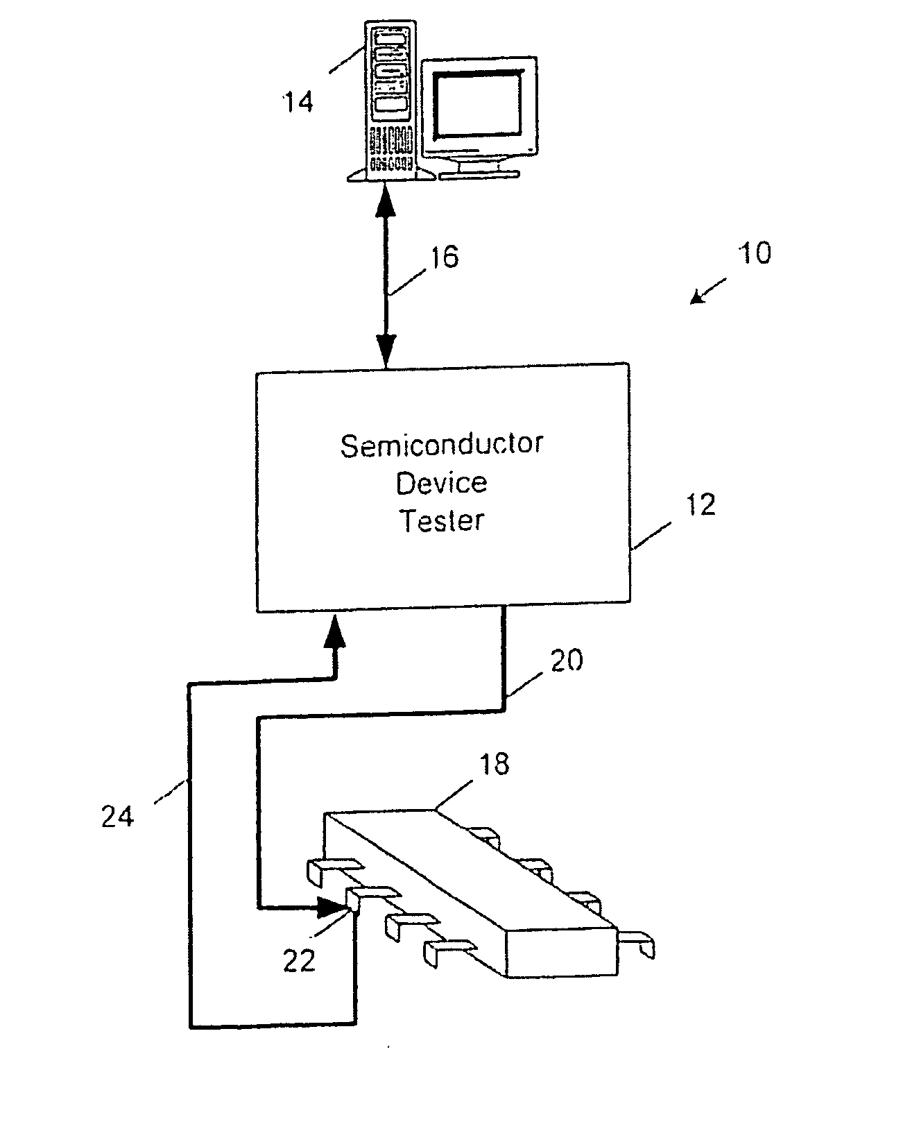
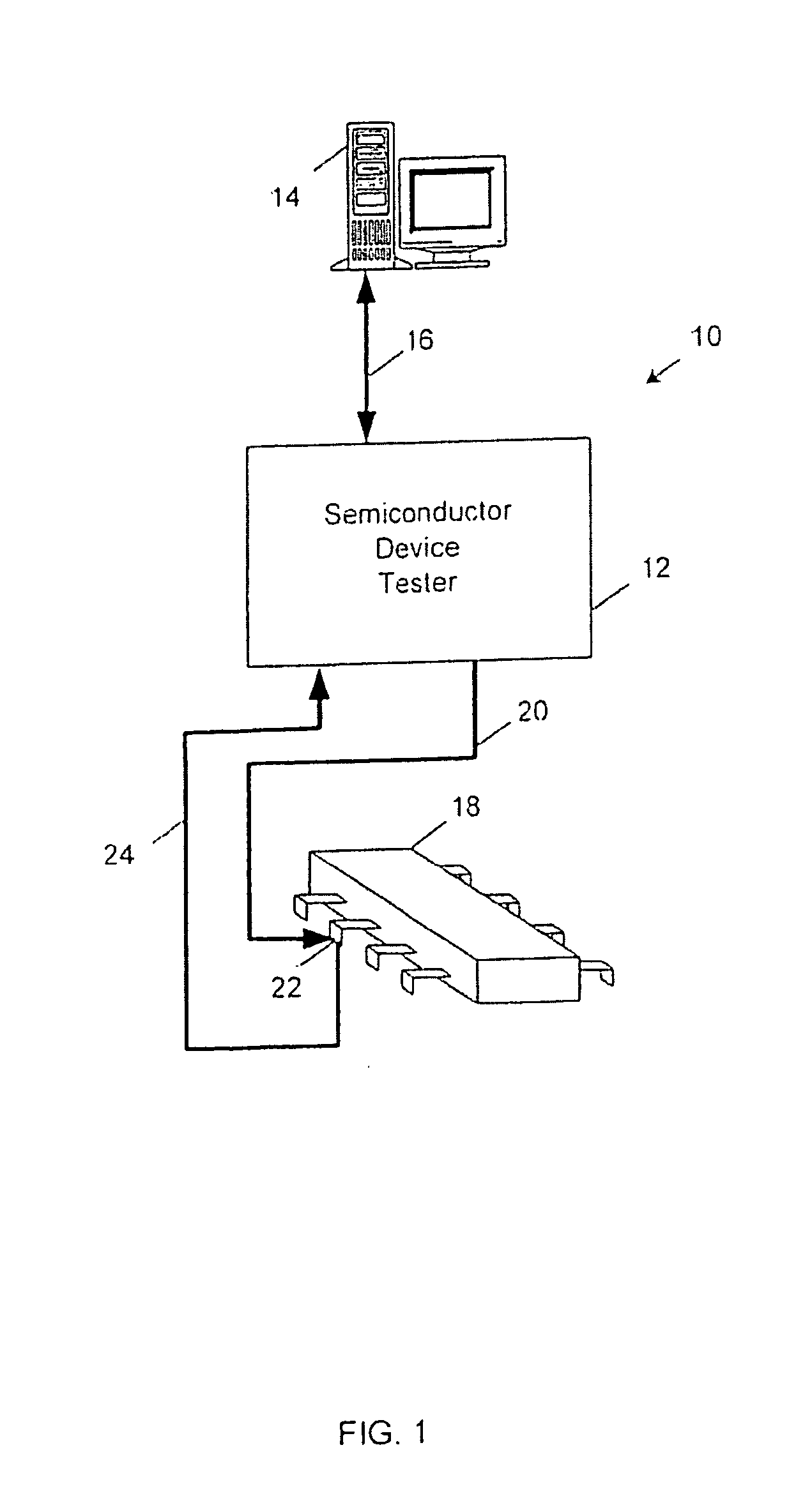
[0017] Referring to FIG. 1, a system 10 for testing semiconductor devices includes a semiconductor device tester 12, such as an ATE or other similar testing device. To control semiconductor device tester 12, system 10 includes a computer system 14 that interfaces with tester 12 over a hardwire connection 16. Typically, computer system 14 provides commands to tester 12 that initiate the execution of routines and functions for testing a semiconductor device. Such executing test routines may initiate the generation and transmission of test signals to the DUT and the collection of responses from the DUT. Various types of semiconductor devices may be tested by system 10. In this example, the DUT is an integrated circuit (IC) chip 18 (e.g., a memory chip, a microprocessor, an analog-to-digital converter, a digital-to-analog converter, etc.).

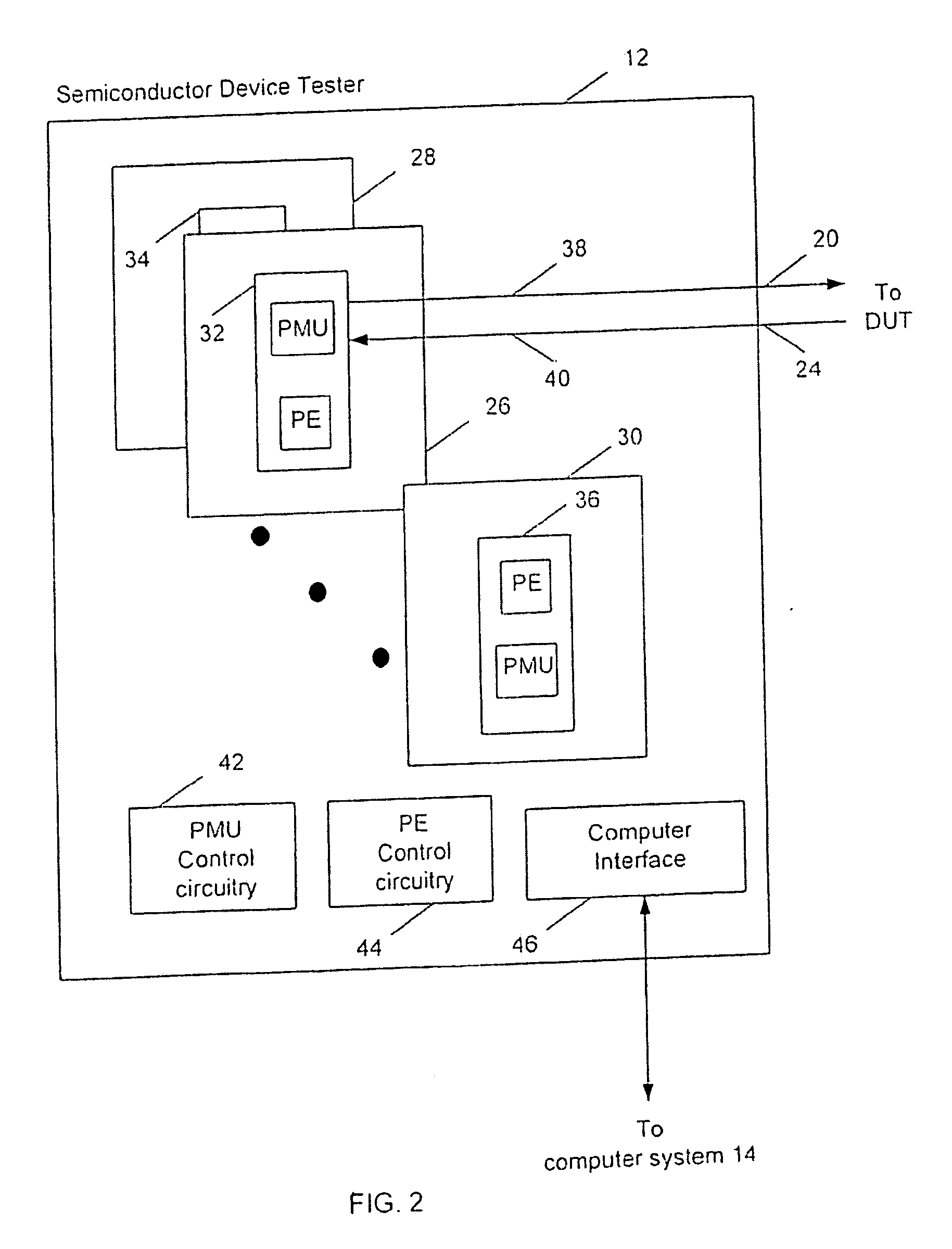
[0018] To provide test signals and collect responses from the DUT, semiconductor device tester 12 is connected to one or more connector pins that pro...


PUM


Abstract

A semiconductor device tester includes a parametric measurement unit (PMU) driver circuit that provides a DC test signal for testing a semiconductor device, and a feedback circuit that senses the DC test signal at an output of the PMU driver circuit and sends the sensed DC test signal to an input of the PMU driver circuit for compensating the DC test signal.

Description

TECHNICAL FIELD [0001] This disclosure relates to the testing of semiconductor devices and, more particularly, to the monitoring of test signals sent to semiconductor devices under test. BACKGROUND [0002] As the commercial demand for semiconductor devices (e.g., memory chips and microprocessors) increases, testing of these devices has become critical for device manufacturers. By testing the semiconductor devices prior to shipping to their customers, defective or under-performing devices may be detected and removed. To perform such tests, semiconductor device testers such as automatic test equipment (ATE) may be used to characterize and validate the performance of manufactured semiconductor devices. [0003] For some types of tests, the ATE may send two types of signals to a device-under-test (DUT). Direct current (DC) signals are sent into the DUT for measuring device characteristics, such as input and output impedance, leakage current, and DUT performance. To produce and send these D...

Claims


Application Information

Patent Timeline
Patent Type & Authority Applications(United States)
IPC IPC(8): G01R31/26
CPCG01R31/31924G11C2029/5602G11C29/56G01R31/3004
Inventor WALKER, ERNEST P.SARTSCHEV, RONALD A.
Owner TERADYNE
Why Eureka
Try Eureka