Method for treating vapor deposition apparatus, method for depositing thin film, vapor deposition apparatus and computer program product for achieving thereof

Inactive Publication Date: 2006-12-14
RENESAS ELECTRONICS CORP
View PDF13 Cites 24 Cited by
  • Summary
  • Abstract
  • Description
  • Claims
  • Application Information

AI Technical Summary

Benefits of technology

[0011] According another aspect of the present invention, there is provided a vapor deposition apparatus for depositing a thin film on a substrate, comprising a chamber capable of being supplied with a vaporized source material of the thin film to deposit the thin film on the substrate; a temperature control unit for controlling a temperature in the chamber; a storage unit that is capable of storing a relationship between a number of the deposition cycles of the thin film and an uniformity in the film thickness of the deposited thin film; a counting unit for counting the number of the deposition cycles of the thin film in the chamber; and a determining unit for comparing the number of the deposition cycles counted by the counting unit with a predetermined number of deposition cycles to determine whether the number of the deposition cycles of the thin film counted by the counting unit is not larger than the predetermined number of the deposition cycles, predetermined number being obtained from the relationship between the number of the deposition cycles of the thin film and the uniformity in the thickness of the thin film, and the relationship being stored in the storage unit, wherein, if the determining unit determines that the number of the deposition cycles is larger than the predetermined number of the deposition cycles, the temperature control unit provides a control of the temperature in the chamber, and an amorphous film is deposited to cover the a

Problems solved by technology

In addition, since the chamber is opened for conducting the wet cleaning process, the level of vacuum created in the chamber must be confirmed after finishing the cleaning process, requiring complicated procedures until a deposition of a thin film is started.
Further, since it is required to elevate the temperature in the chamber to higher temperature after completing the cleaning process and before starting next deposition of a thin film, much time is additionally required for starting next deposition of a thin film, causing another problem.
Since the cleaning process requires much time and the post-cleaning processes also require much time and complicated procedures as de

Method used


Image

  • Method for treating vapor deposition apparatus, method for depositing thin film, vapor deposition apparatus and computer program product for achieving thereof
  • Method for treating vapor deposition apparatus, method for depositing thin film, vapor deposition apparatus and computer program product for achieving thereof
  • Method for treating vapor deposition apparatus, method for depositing thin film, vapor deposition apparatus and computer program product for achieving thereof

Examples


example 1

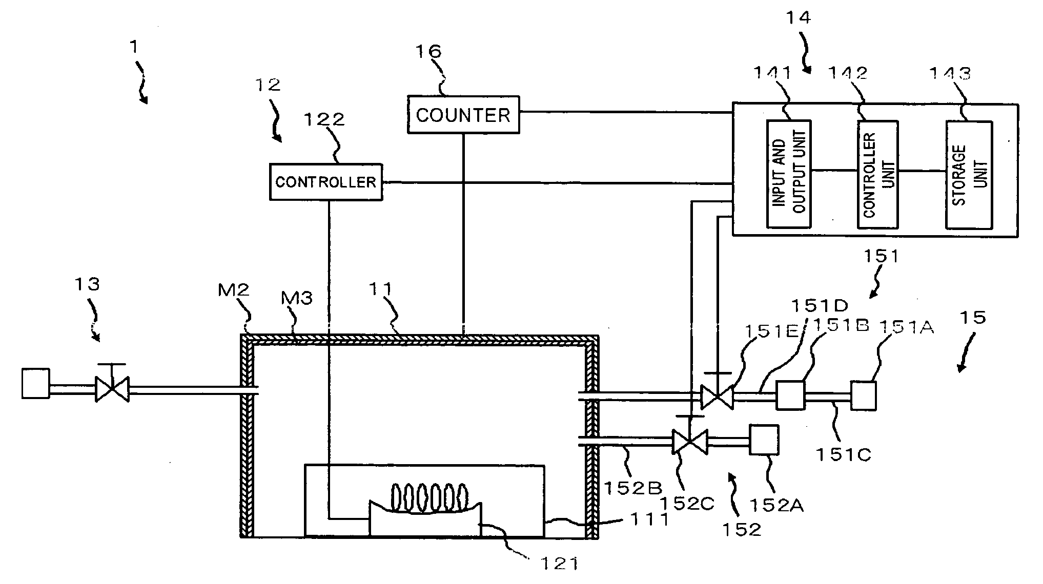
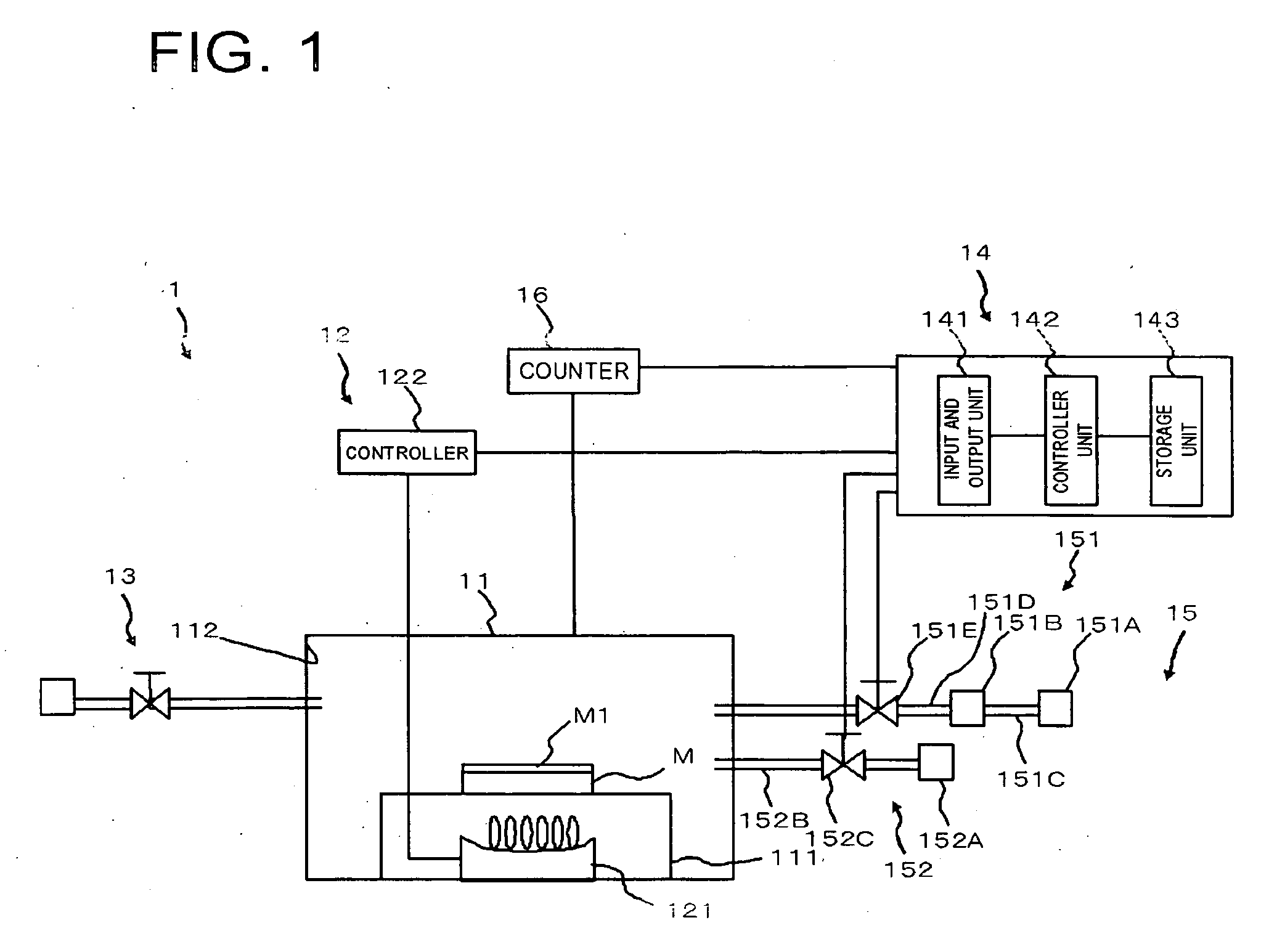
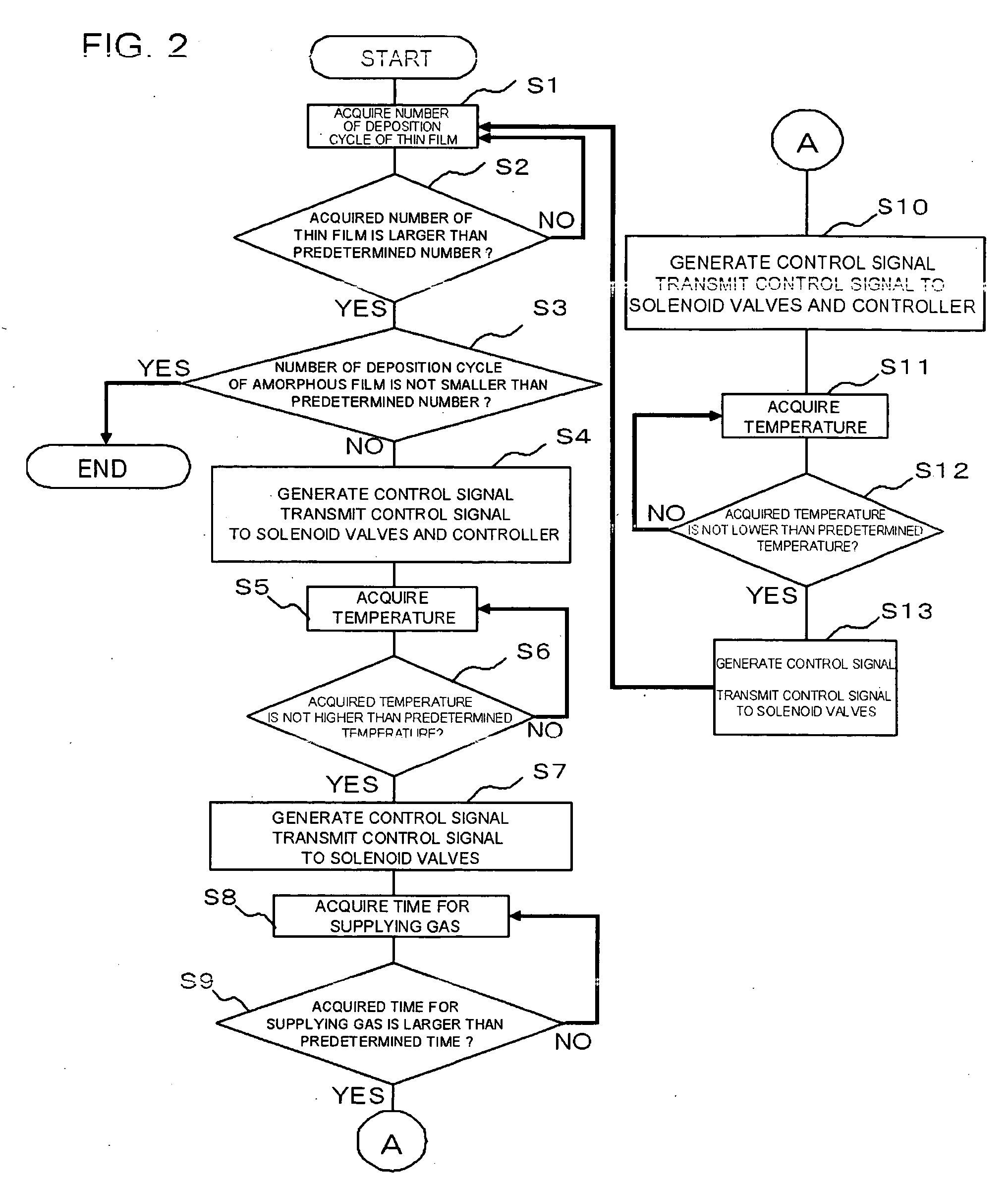
[0052] In example 1, the vapor deposition unit employed in the reference example was also employed, and the source gas and the purge gas employed in reference example were employed to deposit a thin film via an atomic layer epitaxy process. If number of the processed substrates by depositing a thin film was reached to 300 pieces (i.e., critical number of processed substrates for commencing deterioration of the uniformity in the film thickness of the thin film in reference example, (critical number of deposition cycles of the thin film)), the temperature in the chamber was decreased to 200 degree C. Then, the source gas and the purge gas of predetermined volumes, which correspond to depositing 10 thin films, were introduced into the chamber at a temperature of 200 degree C. to deposit an amorphous film of HfO2 on the accumulated material that had been adhered onto the interior wall of the chamber. Here, the temperature in the chamber was decreased, because at least a portion of an am...

example 2

[0054] In example 2, a source gas containing zirconium tetrakis(diethylamide) was employed to deposit a thin film of ZrO2 via an atomic layer epitaxy process. The employed vapor deposition unit and the type of the purge gas were same as employed in example 1. In addition, deposition temperature was set to 270 degree C., and a thickness of a deposited thin film on a substrate was set to 80 angstroms (8 nm). When the number of the processed substrates by depositing the thin film was reached to 300 pieces, the temperature in the chamber was reduced to 200 degree C. Then, the source gas and the purge gas of predetermined volumes, which correspond to depositing 10 thin films, were introduced into the chamber at a temperature of 200 degree C. to deposit an amorphous film of ZrO2 on the accumulated material that had been adhered onto the interior wall of the chamber. When the deposition of the amorphous film was finished, the temperature in the chamber was increased to the deposition tempe...


PUM

PropertyMeasurementUnit
Thicknessaaaaaaaaaa

Abstract

A method for treating a vapor deposition apparatus, a method for depositing a thin film, a vapor deposition apparatus and a computer program product are disclosed for providing a reduced cleaning frequency. Accumulated material is deposited on an interior wall of a chamber of a vapor deposition unit during deposition of a thin film. While the deposition of the thin film is repeated, a gas is emitted from the accumulated material to deteriorate an uniformity in the film thickness of the thin film. The method involves depositing an amorphous film to cover the accumulated material before any influence of the accumulated material deposited on the interior wall of the chamber on the thickness of the thin film is evident. Gas emission from the accumulated material can be prevented by covering the accumulated material with the amorphous film. This configuration provides a thin film having an improved uniformity of thickness.

Description

[0001] This application is based on Japanese patent application No. 2005-173,247, the content of which is incorporated hereinto by reference. BACKGROUND [0002] 1. Field of The Invention [0003] The present invention relates to a method for treating a vapor deposition apparatus, a method for depositing a thin film, a vapor deposition apparatus and a computer program product for achieving thereof. [0004] 2. Related Art [0005] In recent years, it is expected that a high quality thin film having an uniform film thickness is deposited by employing a vapor deposition apparatus. During the deposition process, a source material for the thin film is adhered onto an interior wall of the chamber in the vapor deposition apparatus to form an accumulated material. While the deposition processes are repeatedly conducted in the chamber, the uniformity in the thickness of the deposited thin film is begun to be adversely affected by such accumulated material, thereby deteriorating the uniformity in th...

Claims


Application Information

Patent Timeline
IPC IPC(8): C23C16/00G06F19/00B05C11/00C23C16/44H01L21/316
CPCC23C16/52C23C16/4404
Inventor KATO, YOSHITAKEIWATA, TERUO
Owner RENESAS ELECTRONICS CORP
Why Eureka
Try Eureka