Substrate structure of integrated embedded passive components and method for fabricating the same

a passive component and substrate technology, applied in the field of substrate structure and a method for fabricating the same, can solve the problems of increasing the difficulty and complexity of embedded components, difficult to expand the functions of embedded components, and increasing the cost, so as to prevent the embedded components from being damaged, effective fix the embedded components, and improve the quality of products

Inactive Publication Date: 2006-12-21
ADVANCED SEMICON ENG INC
View PDF6 Cites 20 Cited by
  • Summary
  • Abstract
  • Description
  • Claims
  • Application Information

AI Technical Summary

Benefits of technology

[0012] According to the present invention, the substrate structure of integrated embedded components and a method for fabricating the substrate are provided. Insulating plastic material surrounds the embedded components. Then, it can effectively fix the embedded components and prevent the embedded components from shift and short circuit due to the flow and gather of the melted solder paste after several reflow processes. It can improve the quality of the products, and increase the yield of the products.

Problems solved by technology

In semiconductor processes, the integrated circuits (ICs) manufactured on the same wafer are usually of the same types because to manufacture different types of ICs on the same wafer will increase its difficulty and complexity, and its cost is higher, and it is difficult to expand its functions, and it has the drawbacks of long development time and long test time, etc.
However, in order to meet the requested functions of the electronic products and because their functions cannot be reached by only one IC or only the same types of ICs, it is necessary to integrate different types of components to complete the electronic products with whole functions.
However, the electronic package method often needs at least one reflow process, which is high-temperature process.
The reflow processes will cause the passive components shift due to the melted solder paste, and they will also cause that the passive components cannot be fixed on the bonding pads or misaligned to the locations of the bonding pads.
It will cause some problems happen on the electronic circuits between the passive components and bonding pads.
Furthermore, the melted solder paste on the adjacent bonding pads will flow and gather, and then will cause short circuit.

Method used


Image

  • Substrate structure of integrated embedded passive components and method for fabricating the same
  • Substrate structure of integrated embedded passive components and method for fabricating the same
  • Substrate structure of integrated embedded passive components and method for fabricating the same

Examples


Embodiment Construction

[0016] The detailed description of the present invention will be discussed in the following embodiments, which are not intended to limit the scope of the present invention, but can be adapted for other applications. While drawings are illustrated in details, it is appreciated that the quantity of the disclosed components may be greater or less than that disclosed, except expressly restricting the amount of the components.

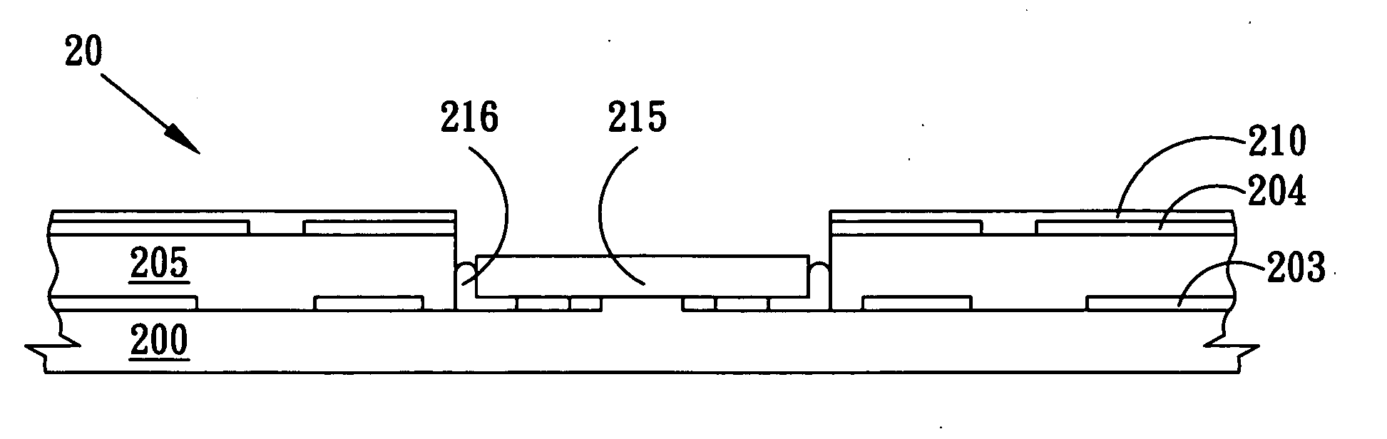
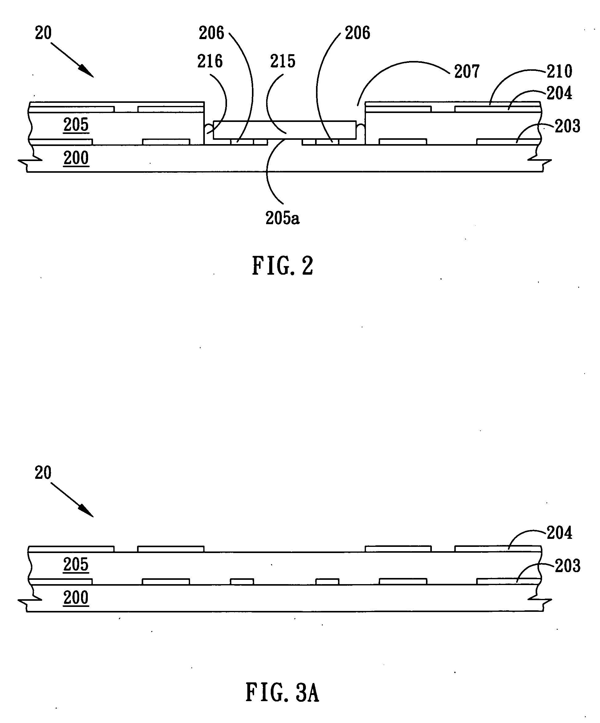
[0017]FIG. 2 shows a cross-sectional diagram of a substrate structure of integrated embedded components according to a preferred embodiment of the present invention. A substrate 20 of integrated components includes a core board 200, on which an inner wiring layer 203 with designed pattern is formed. A dielectric layer 205 is formed on the inner wiring layer 203 to protect the inner wiring layer 203, and an opening 207 in the dielectric layer 205 exposes part of the inner wiring layer 206. Furthermore, an outer wiring layer 204 is formed on the dielectric layer 205....


PUM

PropertyMeasurementUnit
insulatingaaaaaaaaaa
temperatureaaaaaaaaaa
dielectricaaaaaaaaaa

Abstract

The present invention is related to a substrate structure and a method for fabricating the substrate, and more particularly to a substrate structure of integrated embedded passive components and a method for fabricating the substrate. In the present invention, the openings are formed on the substrate by removing part of external circuit layer and part of dielectric layer. Then, the embedded components are disposed in these openings. Therefore, the shift and short circuit of the passive components caused by the flow and gather of the solder paste in reflow or other high-temperature processes can be improved.

Description

BACKGROUND OF THE INVENTION [0001] 1. Field of the Invention [0002] The present invention generally relates to a substrate structure and a method for fabricating the substrate, more particularly to a substrate structure of integrated embedded passive components and a method for fabricating the substrate. [0003] 2. Description of the Prior Art [0004] In semiconductor processes, the integrated circuits (ICs) manufactured on the same wafer are usually of the same types because to manufacture different types of ICs on the same wafer will increase its difficulty and complexity, and its cost is higher, and it is difficult to expand its functions, and it has the drawbacks of long development time and long test time, etc. However, in order to meet the requested functions of the electronic products and because their functions cannot be reached by only one IC or only the same types of ICs, it is necessary to integrate different types of components to complete the electronic products with whol...

Claims


Application Information

Patent Timeline
Patent Type & Authority Applications(United States)
IPC IPC(8): H05K1/16H05K3/30
CPCH05K1/183H05K3/284H05K3/4644H05K3/4697Y10T29/49155H05K2201/10636H05K2201/2036Y10T29/4913H05K2201/09045Y02P70/50
Inventor CHEN, YING-CHOUOU, YING-TELEE, CHIU-WEN
Owner ADVANCED SEMICON ENG INC
Why Eureka
Try Eureka