Side-emitting LED package and manufacturing method of the same

a technology of led packaging and manufacturing method, which is applied in the direction of semiconductor devices, printed circuit aspects, solid-state devices, etc., can solve the problems of inefficiency in productivity, complicated and cumbersome manufacturing process, and limited method for reducing thickness

Active Publication Date: 2006-12-21
SAMSUNG ELECTRONICS CO LTD
View PDF5 Cites 38 Cited by
  • Summary
  • Abstract
  • Description
  • Claims
  • Application Information

AI Technical Summary

Benefits of technology

[0013] The present invention has been made to solve the foregoing problems of the prior art and it is therefore an object of the present invention to provide a side-emitting LED package which does not additionally require an injection-molded material and thus can have minimal thickness, and a manufacturing method of the same.
[0014] It is another object to provide a PCB type side-emitting LED package having a reflecting surface that can easily be manufactured in a desired shape, which can be mass-produced, and a manufacturing method of the same.
[0015] It is further another object to provide a side-emitting LED package which can be mass-produced and is not affected by an LED chip size, and can have an LED array inside thereof, and a manufacturing method of the same.

Problems solved by technology

Aside-emitting LED package 200 illustrated in FIG. 1(a) is a structure, in which a molded body 210 covers a lead frame having an LED chip therein, and thus its thickness is limited to be about 0.5 T. Therefore, such a method is limited in reducing the thickness.
This conventional method, however, entails a complicated process, and thus is not efficient in terms of productivity.
This conventional structure also, however, entails a complicated and cumbersome manufacturing process, in which the retainer 256 and the reflecting surface 258 should be prepared separately to wrap around the lens 254.
However, this conventional technology also bears a problem in that the light transmitting surface 280 is not formed in one particular direction, and thus the reflected light is not focused but tends to be scattered.

Method used


Image

  • Side-emitting LED package and manufacturing method of the same
  • Side-emitting LED package and manufacturing method of the same
  • Side-emitting LED package and manufacturing method of the same

Examples


Embodiment Construction

[0029] Preferred embodiments of the present invention will now be described in detail with reference to the accompanying drawings.

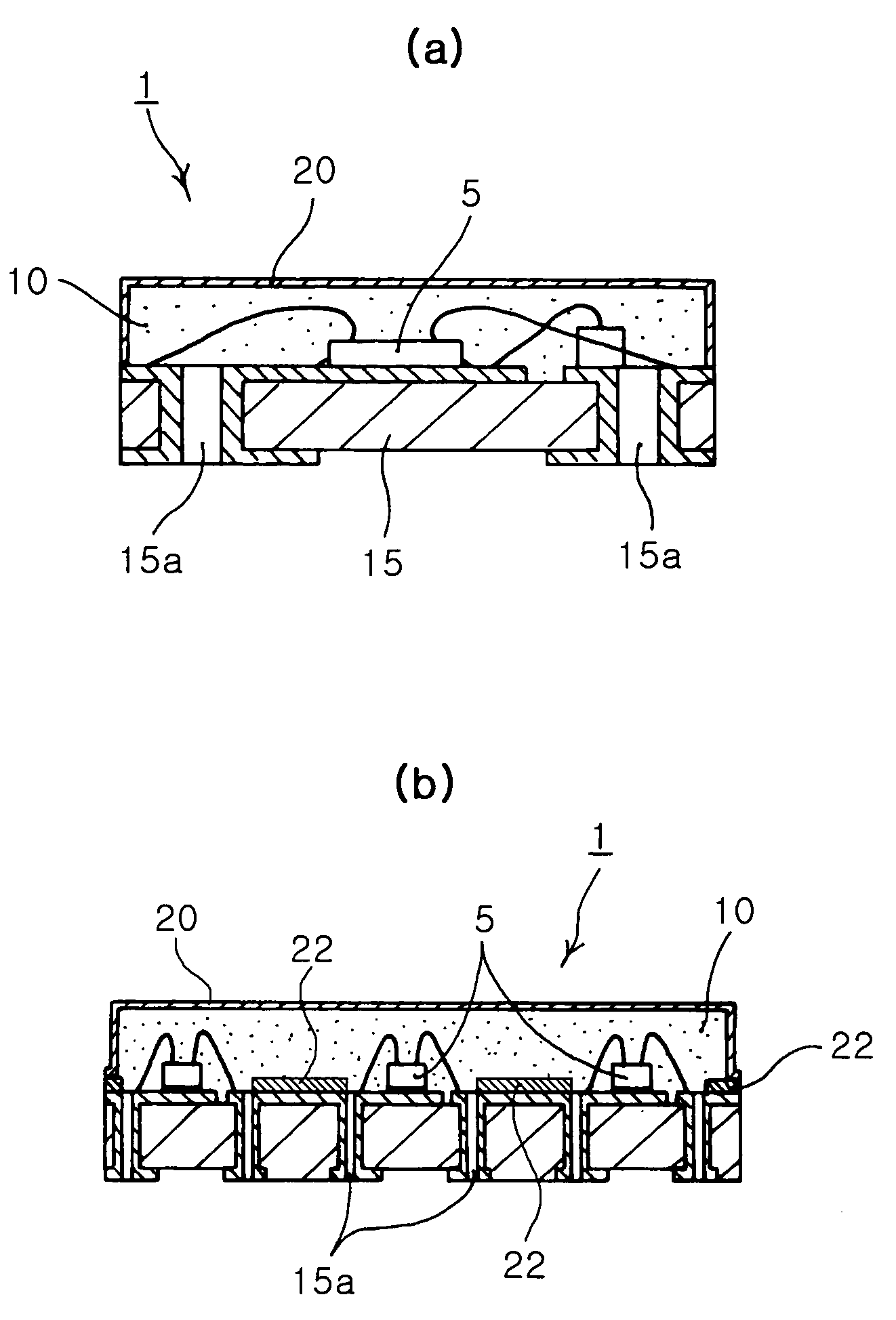
[0030] Referring to FIGS. 3 to 5, a side-emitting LED package 1 according to the present invention is designed to emit light from an LED chip or a light source 5 to one side. The direction of light emission preferably forms a right angle with a plane where the LED chip is mounted.

[0031] The side-emitting LED package 1 according to the present invention has a substrate 15 with electrodes 15a formed thereon. The substrate 15 is preferably a printed circuit board (PCB) or a ceramic substrate having patterned electrodes (not shown) or the electrodes 15a formed as vertical electrodes such as vias.

[0032] In addition, the LED chip as the light source 5 is disposed on the substrate 15 and electrically connected to the electrodes 15a. Either a horizontal type of LED chip having electric terminals formed only on an upper surface thereof or a vertical type of LED...


PUM


Abstract

The invention relates to a side-emitting LED package and a manufacturing method of the same. The invention provides a side-emitting LED package for emitting light from a light source sideward including a substrate with an electrode formed thereon. The package also includes a light source disposed on the substrate, a molded part that covers and protects the substrate with the light source thereon, and a reflective layer that covers an outer surface of the molded part. The molded part with the reflective layer forms a light transmitting surface in one side thereof. The invention allows easy manufacture of a reflecting surface in a desired shape, miniaturization regardless of the LED chip size, mass-production in an LED array, significantly improving productivity.

Description

CLAIM OF PRIORITY [0001] This application claims the benefit of Korean Patent Application No. 2005-46796 filed on Jun. 1, 2005, in the Korean Intellectual Property Office, the disclosure of which is incorporated herein by reference. BACKGROUND OF THE INVENTION [0002] 1. Field of the Invention [0003] The present invention relates to a side-emitting LED package for emitting light from one side thereof, and a manufacturing method of the same. More particularly, the invention relates to a side-emitting LED package which has a reflecting surface easily manufactured in a desired form, can be mass-produced in a compact size regardless of an LED chip size, and can easily be adapted to have an LED array inside thereof, thereby significantly improving productivity, and a manufacturing method of the same. [0004] 2. Description of the Related Art [0005] In general, a backlight such as used in a mobile phone or a PDA adopts an LED package having a light transmitting surface in one side thereof f...

Claims


Application Information

Patent Timeline
Patent Type & Authority Applications(United States)
IPC IPC(8): H01L33/00H01L33/54H01L33/50H01L33/56H01L33/62
CPCH01L25/0753H01L33/0095H01L33/486H01L33/54H01L33/60H01L2224/97H01L2224/32225H01L2224/48091H01L2224/48227H01L2224/73265H05K2201/10106H01L24/97H01L2924/00014H01L2924/00H01L2924/15787H01L2924/181
Inventor HAN, KYUNG TAEGHAHM, HUN JOOKIM, DAE YEONAHN, HO SIKHAN, SEONG YEONPARK, YOUNG SAMLEE, SEON GOO
Owner SAMSUNG ELECTRONICS CO LTD
Why Eureka
Try Eureka