Program method with optimized voltage level for flash memory

Active Publication Date: 2006-12-21
MICRON TECH INC
View PDF13 Cites 92 Cited by
  • Summary
  • Abstract
  • Description
  • Claims
  • Application Information

AI Technical Summary

Benefits of technology

[0009] The various embodiments relate to programming non-volatile memory devices, wherein data is programmed into the array of the memory in a parallel operation, such as the programming of a row of the memory array, and where the programming cycle repeats with increasing programming voltage levels to program any bits of the data that failed to program correctly in the previous cycles. In embodiments of the present invention, the programming voltage of successive programming cycles is increased in relation to the percentage of the data bits that failed programming verification during the previous programming cycle and were not correctly programmed into the memory array. This allows for a faster on average program operation and a more accurate match of the subsequent increase in the programming voltage to the specific non-volatile memory device, the specific region or row being programmed, and any changes in programming characteristics due to device use and wear. In one embodiment of the present invention the manufacturing process/design and/or specific memory device is characterized by generating a failed bit percentage to programming v

Problems solved by technology

Most RAM is volatile, which means that it requires a steady flow of electricity to maintain its contents.
As soon as the power is turned off, whatever data was in RAM is lost.
These programming voltages and/or pulses are typically set by the design and, in certain cases, are trimmed or selected during

Method used


Image

  • Program method with optimized voltage level for flash memory
  • Program method with optimized voltage level for flash memory
  • Program method with optimized voltage level for flash memory

Examples


Embodiment Construction

[0024] In the following detailed description of the preferred embodiments, reference is made to the accompanying drawings that form a part hereof, and in which is shown by way of illustration specific preferred embodiments in which the inventions may be practiced. These embodiments are described in sufficient detail to enable those skilled in the art to practice the invention, and it is to be understood that other embodiments may be utilized and that logical, mechanical and electrical changes may be made without departing from the spirit and scope of the present invention. The following detailed description is, therefore, not to be taken in a limiting sense, and the scope of the present invention is defined only by the claims.

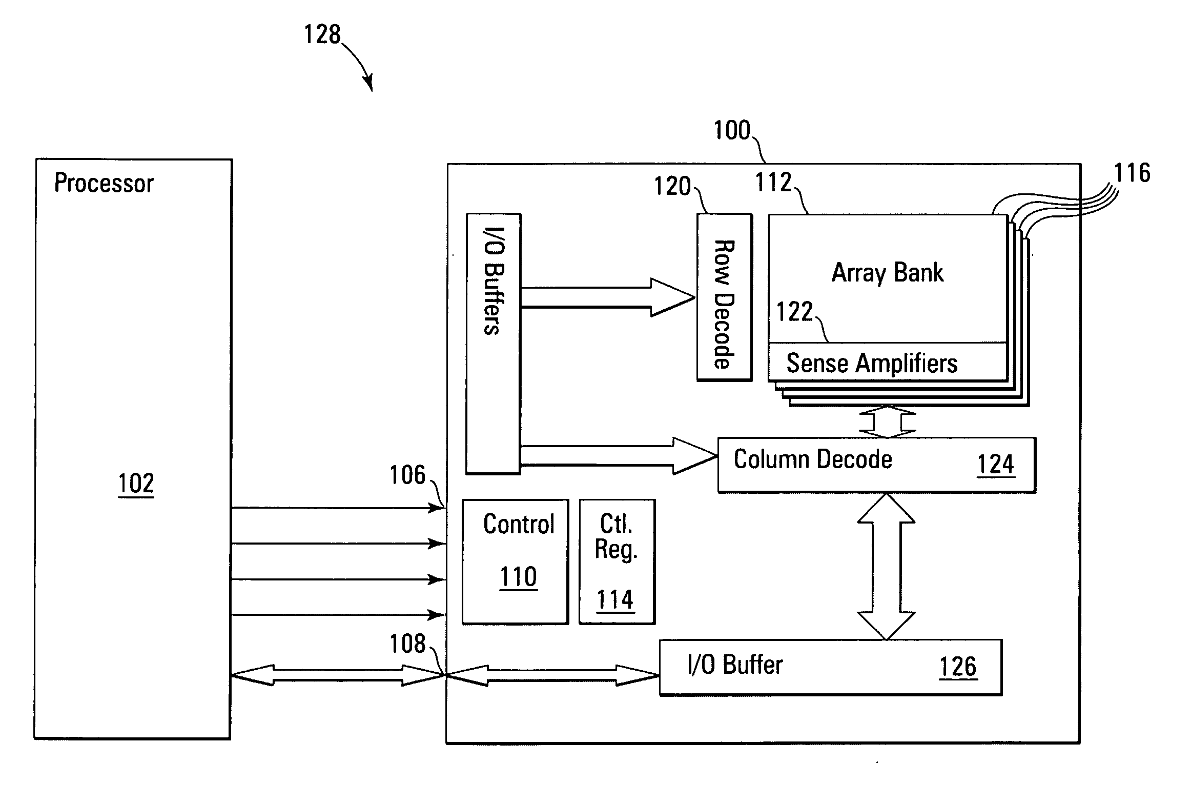
[0025] Embodiments of the present invention include non-volatile memory devices that program data into the non-volatile array in a parallel operation, such as the programming of a row of the memory array, and where the programming cycle repeats with increasing...


PUM


Abstract

A non-volatile memory device and programming process is described that increases the programming voltage of successive programming cycles in relation to the percentage of the data bits that failed programming verification during the previous programming cycle and were not correctly programmed into the memory array. This allows for a faster on average program operation and a more accurate match of the subsequent increase in the programming voltage to the non-volatile memory device, the specific region or row being programmed and any changes due to device wear. In one embodiment of the present invention the manufacturing process/design and/or specific memory device is characterized by generating a failed bit percentage to programming voltage increase profile to set the desired programming voltage delta/increase. In another embodiment of the present invention, methods and apparatus are related for the programming of data into non-volatile memory devices and, in particular, NAND and NOR architecture Flash memory.

Description

TECHNICAL FIELD OF THE INVENTION [0001] The present invention relates generally to memory devices and in particular the present invention relates to Flash memory devices. BACKGROUND OF THE INVENTION [0002] Memory devices are typically provided as internal storage areas in the computer. The term memory identifies data storage that comes in the form of integrated circuit chips. There are several different types of memory used in modern electronics, one common type is RAM (random-access memory). RAM is characteristically found in use as main memory in a computer environment. RAM refers to read and write memory; that is, you can both write data into RAM and read data from RAM. This is in contrast to ROM, which permits you only to read data. Most RAM is volatile, which means that it requires a steady flow of electricity to maintain its contents. As soon as the power is turned off, whatever data was in RAM is lost. [0003] Computers almost always contain a small amount of read-only memory ...

Claims


Application Information

Patent Timeline
IPC IPC(8): G11C16/04
CPCG11C16/3404G11C2029/0409G11C29/028G11C29/021G11C16/34G11C16/12
Inventor HA, CHANG WAN
Owner MICRON TECH INC
Why Eureka
Try Eureka