Magnetic shielding of MRAM chips

a technology of magnetic shielding and mram chips, applied in the direction of digital storage, semiconductor/solid-state device details, instruments, etc., can solve the problems of affecting the orientation of the magnetic field of the mram memory device, memory may record wrong states, unwanted electromagnetic pulses of wide dynamic range, etc., and achieves the effect of lowering the cost and improving the shielding

Inactive Publication Date: 2006-12-28
ALTIS SEMICON +1
View PDF3 Cites 44 Cited by
  • Summary
  • Abstract
  • Description
  • Claims
  • Application Information

AI Technical Summary

Benefits of technology

[0015] An advantageous feature of the present invention is that no customized MRAM chip packaging is required and thus cost is lowered. Another advantageo

Problems solved by technology

The orientation of the magnetic fields of the MRAM memory device, however, may be affected by external magnetic fields.
Undesired external magnetic fields may change the orientation of the MRAM memory so that the memory may record wrong states.
Other unwanted fields including electromagnetic pulses of wide dynamic range can be caused by local severe thunderstorms and improperly groun

Method used


Image

  • Magnetic shielding of MRAM chips
  • Magnetic shielding of MRAM chips
  • Magnetic shielding of MRAM chips

Examples


Embodiment Construction

[0027] The making and using of the presently preferred embodiments are discussed in detail below. It should be appreciated, however, that the present invention provides many applicable inventive concepts that can be embodied in a wide variety of specific contexts. The specific embodiments discussed are merely illustrative of specific ways to make and use the invention, and do not limit the scope of the invention.

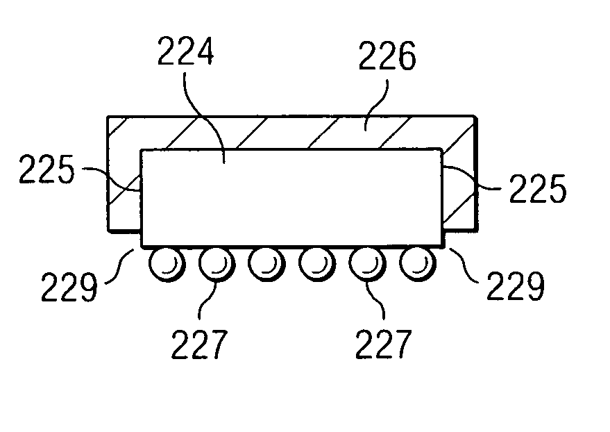
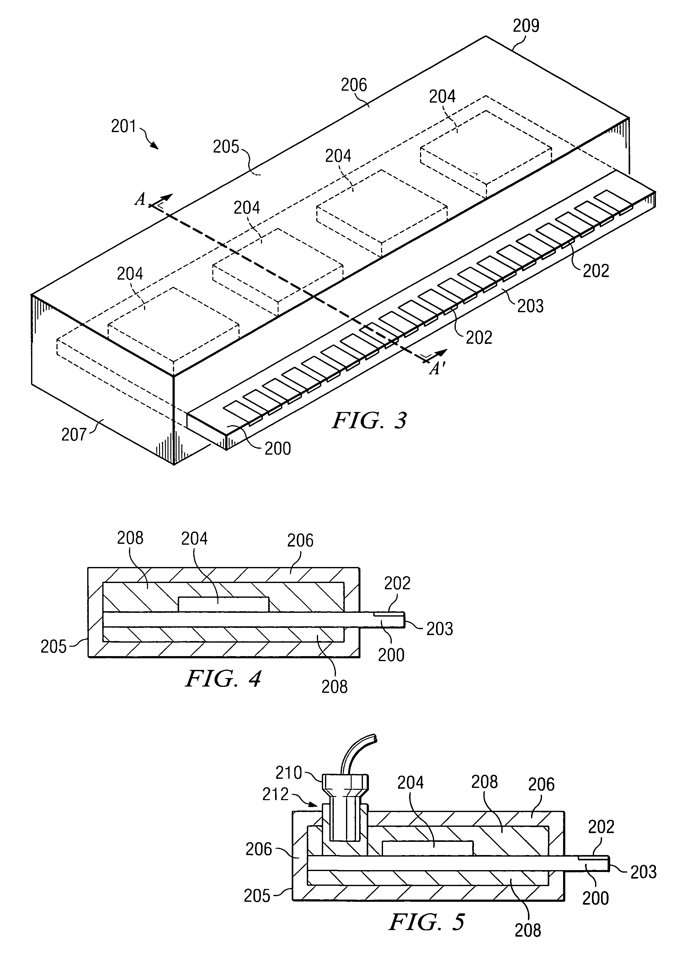
[0028]FIG. 3 illustrates a preferred embodiment of the present invention. Memories are often used in the form of memory modules. Throughout the description, the term “memory module” is used to refer to any circuit board that has at least one memory chip, even if the memory chip is not a main component. Thus, besides memory chips 204, a memory module may also contain other circuit components. A memory module 201 includes MRAM chips 204 attached to the topside of a circuit board 200, which typically has four ends 203, 205, 207 and 209. The MRAM chips 204 can be packaged using...


PUM


Abstract

An apparatus comprising a magnetically shielded MRAM chip and a method of manufacturing the same. The apparatus includes an MRAM module and a protective cover. The MRAM module includes a circuit board and a memory chip attached to the circuit board, the memory chip containing magnetoresistive random access memory (MRAM) cells. The protective cover includes a magnetic shielding material and at least partially encloses the memory chip. In another embodiment, the protective cover shields the memory chip without shielding at least a portion of the circuit board.

Description

TECHNICAL FIELD [0001] The present invention relates generally to magnetoresistive random access memory (MRAM) devices, and more particularly to magnetic shielding of MRAM chips. BACKGROUND [0002] Semiconductors are used in integrated circuits for electronic applications, including radios, televisions, cell phones, and personal computing devices, as examples. One type of semiconductor device is a semiconductor storage device, such as a dynamic random access memory (DRAM) or a flash memory, both of which use charge to store information. [0003] A more recent development in semiconductor memory devices involves spin electronics, which combines semiconductor technology and magnetic materials and devices. The spins of electrons, through their magnetic moments, rather than the charge of the electrons, is used to indicate the presence of a “1” or “0”. One such spin electronic device is a magnetoresistive random access memory (MRAM), sometimes referred to as magnetic RAM, device 100, as sho...

Claims


Application Information

Patent Timeline
IPC IPC(8): H01L23/552
CPCG11C11/15H01L23/29H01L2924/3025H01L2224/16H01L23/552
Inventor GOGL, DIETMARBRAUN, DANIEL
Owner ALTIS SEMICON
Why Eureka
Try Eureka