
Memory element conducting structure

a technology of conducting structure and memory element, applied in the direction of basic electric elements, solid-state devices, instruments, etc., can solve the problems of increasing the difficulty of improving the yield rate, waste of time in the examination procedure of memory modules, and the need to unsolder memory elements for further examination, etc., to achieve convenient replacement of the repair of the defective memory elemen

Inactive Publication Date: 2006-12-28
OPTIMUM CARE INT TECH
View PDF6 Cites 1 Cited by
  • Summary
  • Abstract
  • Description
  • Claims
  • Application Information

AI Technical Summary

Benefits of technology

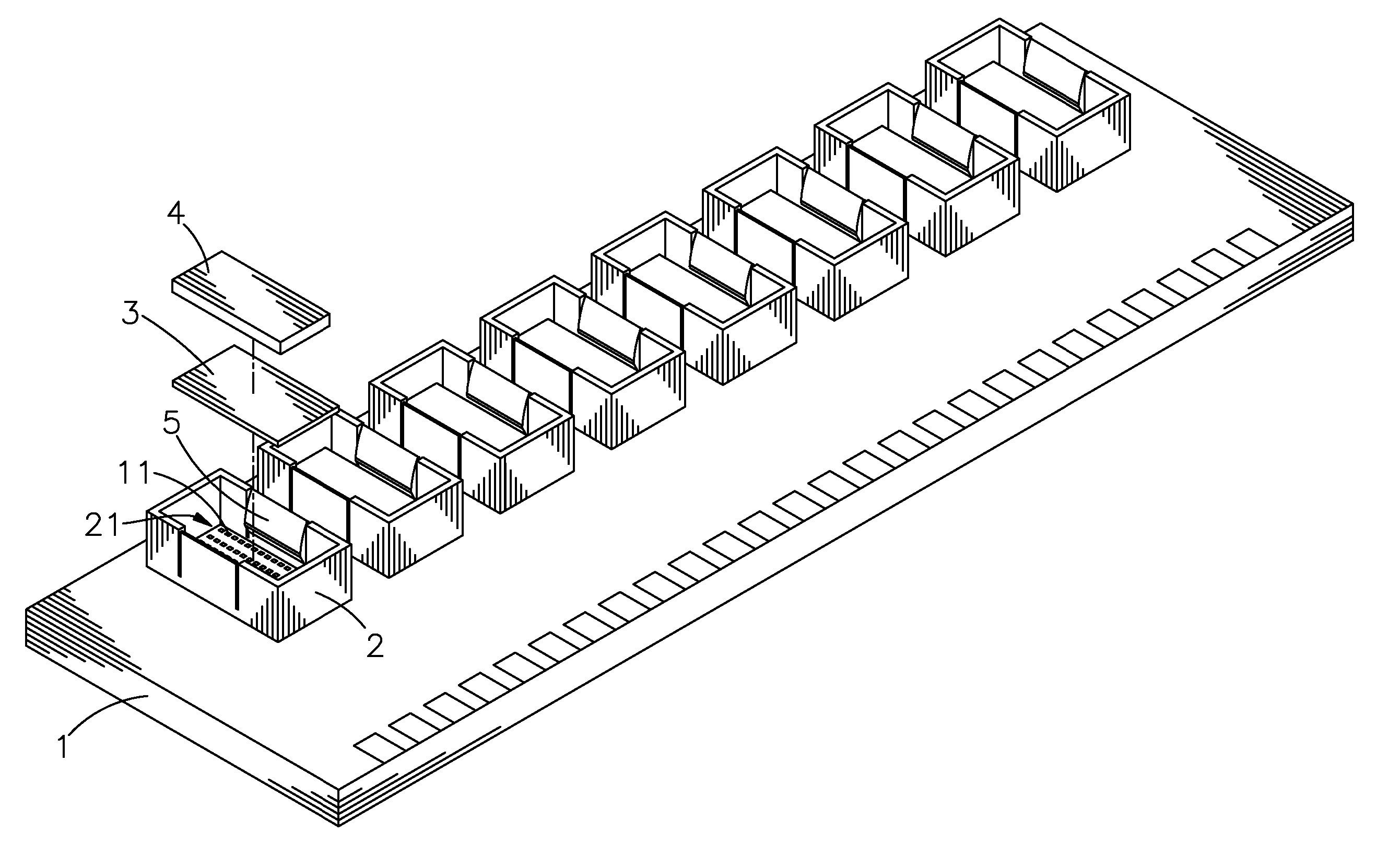
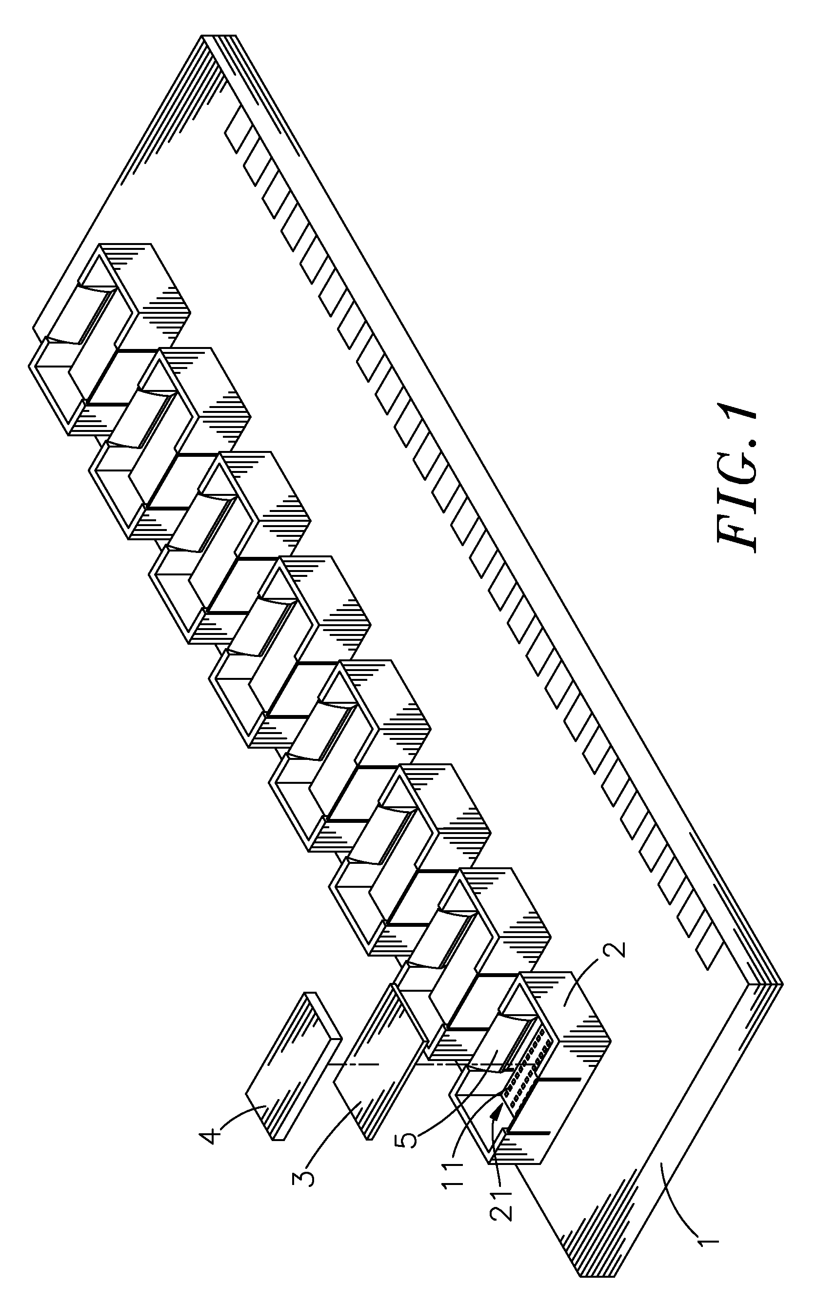
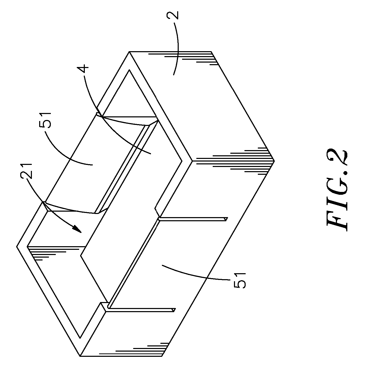
[0009] The present invention has been accomplished under the circumstances in view. According to one aspect of the present invention, the memory element conducting structure comprises a substrate, which has a control circuit arranged therein and a plurality of contacts provided at a top side thereof and electrically connected to the control circuit, at least one hollow socket respectively provided at the top side of the substrate corresponding to the contacts of the substrate, each hollow socket defining therein a holding space corresponding to the contacts of the substrate, at least one conductive medium respectively mounted in the at least one hollow socket and pressed on the contacts of the substrate, and at least one positioning means respectively provided in the at least one hollow socket and adapted to hold down a memory element having a plurality of circuit contacts in each of the at least one hollow socket and to impart a downward pressure to the memory element in each of the at least one hollow socket against the conductive medium in each of the at least one hollow socket and the respective contacts of the substrate for enabling the control circuit of the substrate to control the operation of the memory element being set in each of the at least one hollow socket. According to another aspect of the present invention, when one memory element in one hollow socket is tested to be defective, the positioning means at each of the respective hollow socket can conveniently be disengaged from the defective memory element, allowing convenient replacement of repair of the defective memory element.

Problems solved by technology

However, this memory module examination procedure wastes much time.
When an error occurred during the test of one memory module, the memory elements of the memory module must be unsoldered for further examination individually.
Following the market trend toward relatively smaller size in the fabrication of electronic products, the requirement for manufacturing precision is critical, and improvement in yield rate has become a great challenge.
In consequence, the repair work of defective products is frequently encountered in factory.

Method used


Image

  • Memory element conducting structure
  • Memory element conducting structure
  • Memory element conducting structure

Examples


second embodiment

[0034] FIGS. 6A˜6C show the present invention. According to this embodiment, each positioning means 5 comprises a cover plate 52 on the respective hollow socket 2 and adapted to close the holding space 21 of the respective hollow socket 2, a hook 522 extended from one end (the free end) of the cover plate 52 for hooking in a hook hole 23 at the respective hollow socket 2 to lock the cover plate 52 to the respective hollow socket 2 in the closed position, and a holding-down means 521 provided at the inner side of the cover plate 52 for holding down the respective memory element 4 in the holding space 21 of the respective hollow socket 2. The holding-down means 521 can be a protruding portion 5211 projecting from the inner wall of the cover plate 52 as shown in FIG. 6A, a holding-down spring 5212 fixedly mounted on the inner wall of the cover plate 52 as shown in FIG. 6B, or a smoothly curved holding-down wall portion 523 as shown in FIG. 6C. Further, the size of the protruding portio...

third embodiment

[0035] FIGS. 7A˜7C show the present invention. According to this embodiment, each positioning means 5 comprises a detachable cover plate 53 that is detachably fastened to the respective hollow socket 2 to close the holding space 21, a plurality of male retaining portions 532 provided at the detachable cover plate 53 for engaging into respective retaining holes 24 at the respective hollow socket 2 to lock the detachable cover plate 53 to the respective hollow socket 2, and holding-down means 531 provided at the inner side of the detachable cover plate 53 for holding down the respective memory element 4 in the holding space 21 of the respective hollow socket 2. The holding-down means 531 can be protruding portions 5311 projecting from the inner wall of the detachable cover plate 53 as shown in FIG. 7A, a holding-down spring 5312 fixedly mounted on the inner wall of the detachable cover plate 53 as shown in FIG. 7B, or a smoothly curved holding-down wall portion 533 as shown in FIG. 7C...

fourth embodiment

[0036]FIGS. 8A and 8B show the present invention. According to this embodiment, each positioning means 5 comprises two springy hooks 55 symmetrically provided at the two opposite lateral sides of the respective hollow socket 2. When inserting the memory element 4 into the holding space 21 of the hollow socket 2, the two springy hooks 55 are respectively forced outwards for allowing the memory element 4 to pass to the bottom side in the holding space 21 of the hollow socket 2. After the memory element 4 has been set into position in close contact with the conducting medium 3 against the contacts 11 of the substrate 1 in the holding space 21 of the respective hollow socket 2, the springy hooks 55 immediately return to their former shape to hook on the top wall of the memory element 4, imparting a downward pressure to the memory element 4 against the conducting medium 3 and the contacts 11 of the substrate 1. When wishing to take the memory element 4 out of the respective hollow socket...


PUM


Abstract

Disclosed is a memory element conducting structure, which includes a substrate with contacts, hollow sockets provided at the top side of the substrate corresponding to the contacts of the substrate, conducting media respectively mounted in the hollow sockets and supported on the contacts, and a plurality of positioning means respectively provided in the hollow sockets for holding down a respective memory element against the conducting medium in each hollow socket and the respective contacts of the substrate for enabling a control circuit of the substrate to control the operation of each memory element.

Description

[0001] This application claims the priority benefit of Taiwan patent application number 094210733 filed on Jun. 24, 2005. BACKGROUND OF THE INVENTION [0002] 1. Field of the Invention [0003] The present invention relates generally to memory element conducting arrangements and more particularly, to a memory element conducting structure, which uses positioning means to hold down a memory element in a respective hollow socket against a respective conductive medium and the respective contacts of a substrate for enabling a control circuit of the substrate to control the operation of the memory element. [0004] 2. Description of the Related Art [0005] Following fast development of electronic technology, a variety of electronic products have been continuously developed and intensively used in our daily life to improve the living quality. Many electronic products, such as computers, communication devices and etc., use memory means for storing and exchanging data. [0006] After the fabrication ...

Claims


Application Information

Patent Timeline
Patent Type & Authority Applications(United States)
IPC IPC(8): H01L23/02G11C29/00H01L21/60
CPCG01R1/0483H01L23/32H01L2924/00011H01L2224/293H01L2224/2929H01L2924/01033H01L2224/83851H01L2224/838H01L2224/16H01L23/49827H01L24/72H01L24/83H01L24/90H01L25/0655H01L2224/29075H01L2924/00014H01L2224/81901H01L2224/73251H01L2224/72H01L2224/0401
Inventor LIEN, SHIH-HSIUNG
Owner OPTIMUM CARE INT TECH
Learn More