Electronic part test device

a technology of electronic parts and test equipment, applied in the direction of measurement devices, semiconductor/solid-state device testing/measurement, instruments, etc., can solve the problems of inability to increase the efficiency of tests, the normal operation of ccd cameras cannot be expected, and the exchange time when changing the type of ic chips cannot be shortened, so as to achieve fast positioning and improve test efficiency.

Inactive Publication Date: 2006-12-28
ADVANTEST CORP
View PDF14 Cites 39 Cited by
  • Summary
  • Abstract
  • Description
  • Claims
  • Application Information

AI Technical Summary

Benefits of technology

[0042] By having the moving means pick up the DUTs in the state constrained in planar motion by the recesses or other constraining means and having the moving means move the DUTs from the constraining means to the holding surfaces of the test plate, instead of the positioning by the above image processing, mechanical positioning of the DUTs by the constraining means becomes possible when placing the DUTs on the holding surfaces of the test plate. This mechanical positioning enables the DUTs to be quickly moved to the holding surfaces of the te

Problems solved by technology

Therefore, in a memory IC test apparatus using such test trays, the exchange time when changing types of IC chips cannot be shortened.
In particular, it is not possible to increase the efficiency of tests when testing small amounts of a variety of types of devices.
Normal

Method used


Image

  • Electronic part test device
  • Electronic part test device
  • Electronic part test device

Examples


first embodiment

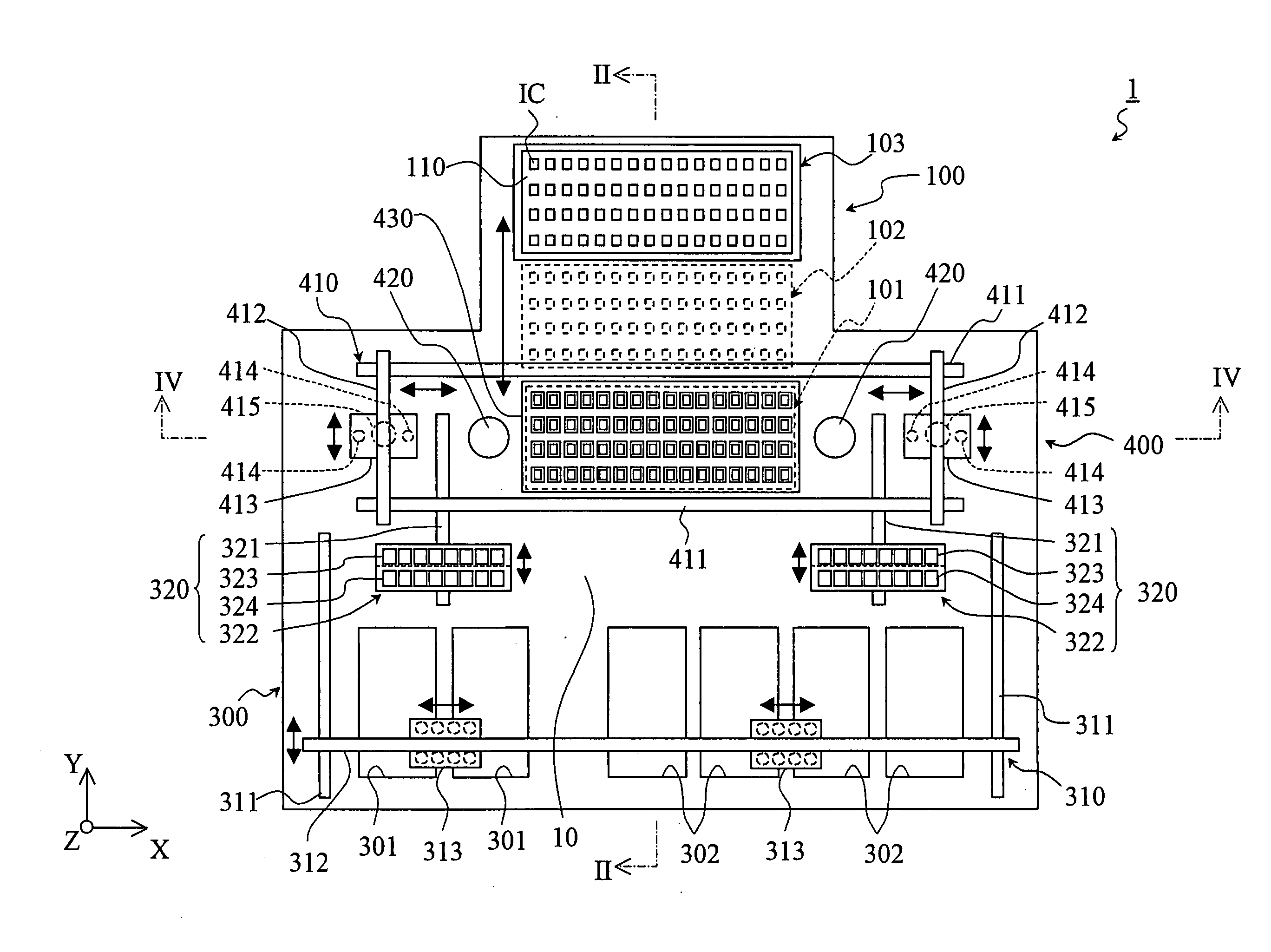
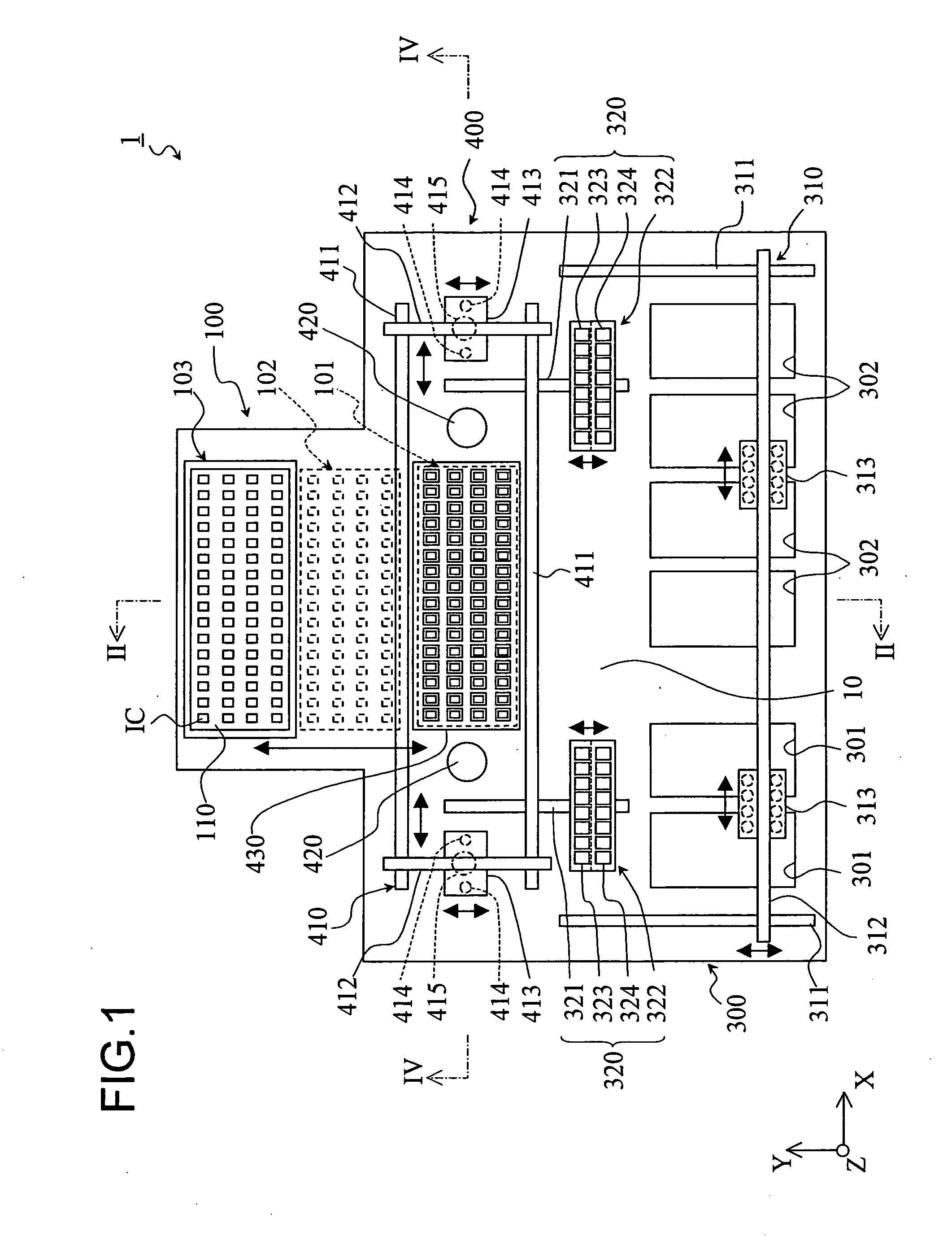
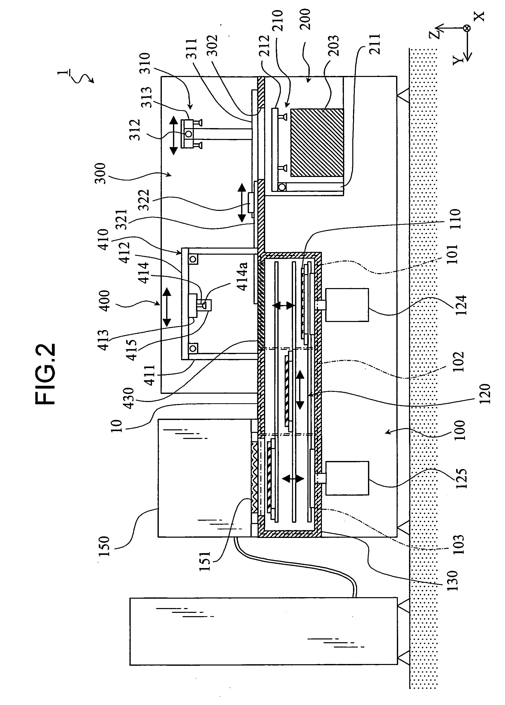
[0075] The electronic device test apparatus 1 of the present invention holds a plurality of (in the present embodiment, 64) IC chips (in FIG. 1 to FIG. 28B, shown by notations “IC”) on a test plate 110, conveys them to contact units 151 provided at a test head 150 for simultaneous testing in that state, and classifies the IC chips and stores them on predetermined trays according to the test results after the testing. It tests the devices under test, that is, the IC chips, in a state given thermal stress in a state of temperature higher than ordinary temperature (high temperature) or a state of temperature lower than ordinary temperature (low temperature).

[0076] As shown in FIG. 1, FIG. 2, and FIG. 3, the electronic device test apparatus 1 of the present embodiment is comprised of an IC stocker unit 200 for storing the IC chips to be test and classifying and storing the after-test IC chips, a loader / unloader unit 300 for feeding before-test IC chips supplied from the IC stocker unit ...

third embodiment

[0095] The movable head 322 of each second IC conveyor system 320 is provided with a supply holder 323 for holding before-test IC chips and an eject holder 324 for holding after-test IC chips. The supply holder 323 and eject holder 324 respectively have eight recesses 323b with outwardly slanted edges and are designed to be able to hold eight IC chips under test. In general, IC chips carried on a customer tray greatly vary in position, but by forming recesses 323b in the supply holder 323, when the movable head 313 of the first IC conveyor system 310 drops the before-test IC chips into the recesses, their slanted surfaces correct the dropped positions of the IC chips whereby the positions and postures are corrected so that the eight before-test IC chips are correctly set. Note that the recesses 323b of the holders 323, 324 do not constrain the planar motion of the IC chips like the recesses 323b′ of the later explained third embodiment and are formed with a large margin compared wit...


PUM


Abstract

An electronic device test apparatus for testing IC chips (IC) by pushing their input/output terminals (HB) against contact units of a test head, provided with a test plate (110) compraised holders (113) for holding back surfaces of IC chips (IC) where no input/output terminals (HB) are led out with substantially smooth holding surfaces (114) larger than those back surfaces, and the test plate body (111) for holding the holders (113) in a manner rockable at the time of testing, the side surfaces (113b) of the holders (113) being guided by guide surfaces (153) provided in the vicinities of contact units (151) and the IC chips (IC) held by the holders (113) being pushed against contact pins of the contact units (151).

Description

BACKGROUND OF THE INVENTION [0001] 1. Field of the Invention [0002] The present invention relates to an electronic device test apparatus for testing semiconductor integrated circuit devices and various other electronic devices (hereinafter also referred to representatively as “IC chips”), more particularly relates to an electronic device test apparatus enabling a large number of types of electronic devices under test (“DUTs”) to be easily handled. [0003] 2. Description of the Related Art [0004] In an IC test apparatus (electronic device test apparatus) called a “handler”, a large number of IC chips stored on a tray are conveyed inside the handler, the IC chips are brought into electrical contact with a test head, and the electronic device test apparatus unit (hereinafter, also referred to as a “tester”) is made to conduct the tests. Further, after the tests are completed, the IC chips are ejected from the test head and transferred onto a tray in accordance with the test results to t...

Claims


Application Information

Patent Timeline
IPC IPC(8): G01R31/26G01R31/28
CPCG01R31/2886G01R31/2893G01R31/2887G01R31/26H01L22/00
Inventor YAMASHITA, KAZUYUKIITO, AKIHIKO
Owner ADVANTEST CORP
Why Eureka
Try Eureka