
Semiconductor integrated circuit device

a technology of integrated circuits and semiconductors, applied in the direction of power consumption reduction, pulse techniques, instruments, etc., can solve the problems of indefinite signal propagation prevention design complexity, signal wiring in the chip, and increase in shutdown variations, so as to facilitate power shutdown control inside the chip

Active Publication Date: 2006-12-28
RENESAS ELECTRONICS CORP
View PDF1 Cites 21 Cited by
  • Summary
  • Abstract
  • Description
  • Claims
  • Application Information

AI Technical Summary

Benefits of technology

The patent text describes a problem in designing a system-on-chip (SoC) that includes multiple power domains and independently controls power shutdown. The challenge is to prevent leakage currents and uncertainties in signal propagation between power domains while also ensuring high-speed recovery from power shutdown. Other issues include the need for a repeater to prevent unsharpened signal waveform and the difficulty in distributing clock signals. The patent text proposes solutions to address these challenges.

Problems solved by technology

In the case where power shutdown is independently controlled respectively, some problems occur as to signal wiring in the chip.
Power shutdown variations increase in number, and an indefinite signal propagation prevention design becomes complicated.
However, if a voltage of an intermediate value between these signals is inputted, there is a tendency that a large penetration current is fed.
If there occurs a plurality of variations, a control method becomes complicated.
Thus, there is a fear that a design is not closed within a limited designing period.
Therefore, there is a tendency that a chip also becomes large in size.
Thus, a time constant of a signal represented by a product thereof becomes large, a transmission delay is degraded, and an unsharpened signal waveform is generated.

Method used


Image

  • Semiconductor integrated circuit device
  • Semiconductor integrated circuit device
  • Semiconductor integrated circuit device

Examples


first embodiment

[0075] (First Embodiment)

[0076] With reference to FIG. 1 to FIG. 5, a description will be given with respect to a first embodiment relating to a semiconductor integrated circuit device according to the present invention.

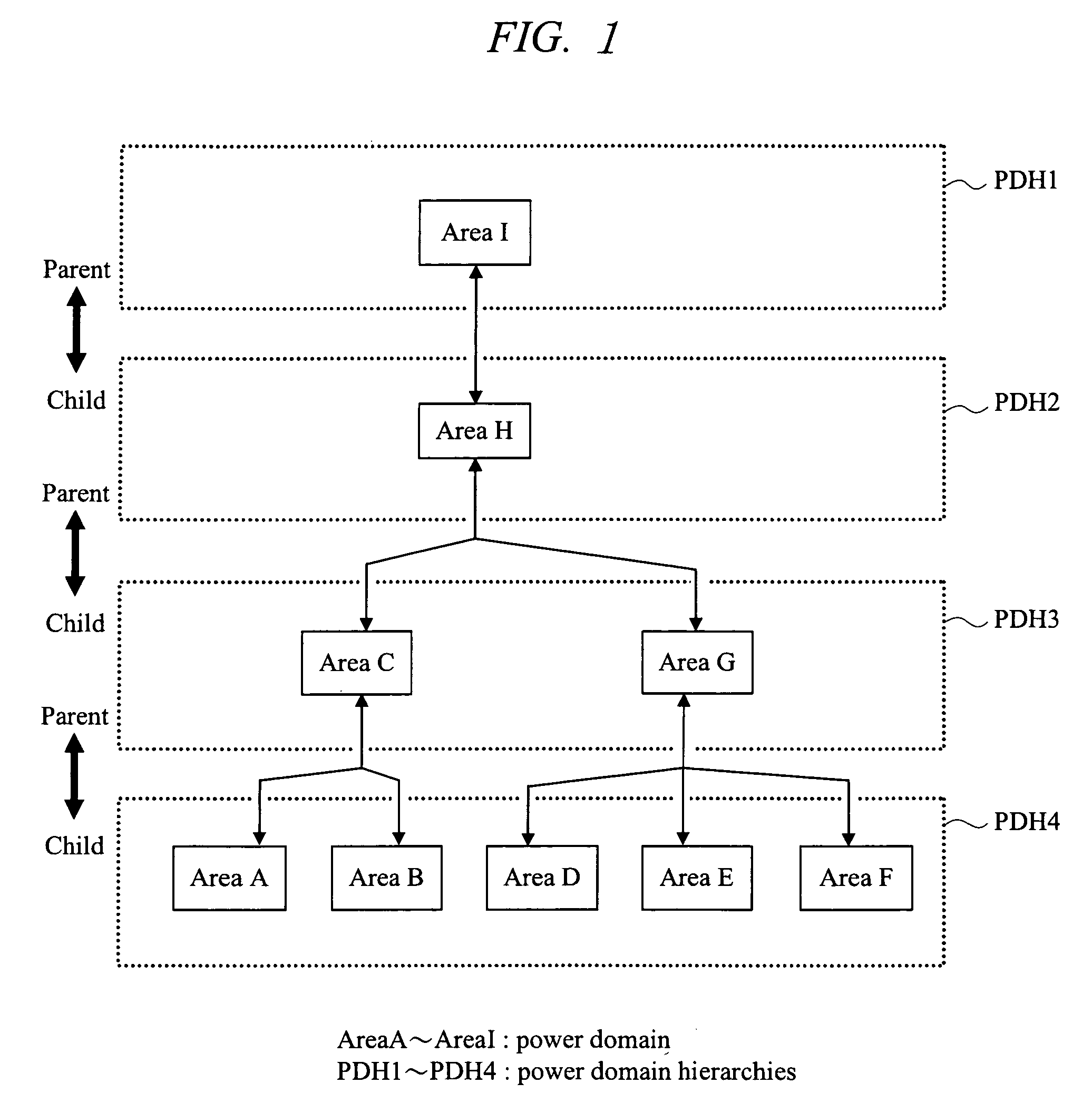
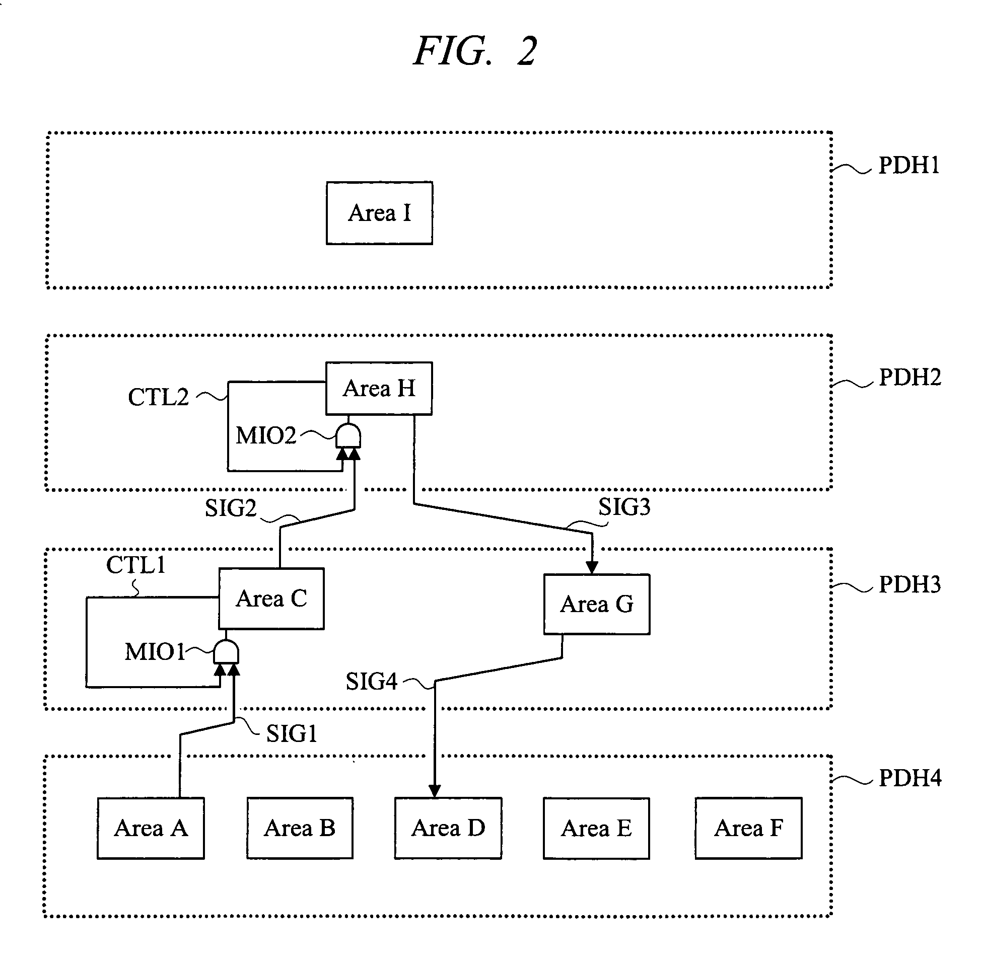
[0077]FIG. 1 is a view showing a method for configuring power domains with respect to a case in which four power domain hierarchies and nine independent power domains are assumed to exist inside of an SoC as an example of a hierarchy of independent power interrupt areas. These independent power domains are operated by a high voltage power supply and a ground power supply that is different from the high voltage power supply and a power supply used in other power domains, and the respectively different ground power supplies are supplied independently each other. In addition, in these power domains, control of power shutdown can be achieved independently each other; the power shutdown priorities are assigned respectively; the priorities are associated with each other b...

second embodiment

[0096] (Second Embodiment)

[0097] With reference to FIG. 6 and FIG. 7, a description will be given with respect to a second embodiment relating to a semiconductor integrated circuit device according to the present invention.

[0098]FIG. 6 is a view showing an example in which power domains described in FIG. 1 to FIG. 5 are packaged on a SoC (System-on-Chip) as an example of a case in which independent power shutdown areas have been mounted on a chip. Here, there is shown an example of division into nine power domains from Area A to Area I shown in FIG. 1 to FIG. 5. In addition, in FIG. 6, small sized power domains indicated by SPA1 to SPA10 are defined as Area H. These small sized power domains are referred to as subsidiary power domains. This subsidiary power domain is provided as an independent power domain having a low power shutdown priority, as shown in the hierarchy of FIG. 1, as is evident from the fact that the area is defined as Area H. In these power domains, power is shut d...

third embodiment

[0105] (Third Embodiment)

[0106] With reference to FIG. 8 and FIG. 9, a description will be given with respect to a third embodiment relating to a semiconductor integrated circuit device according to the present invention.

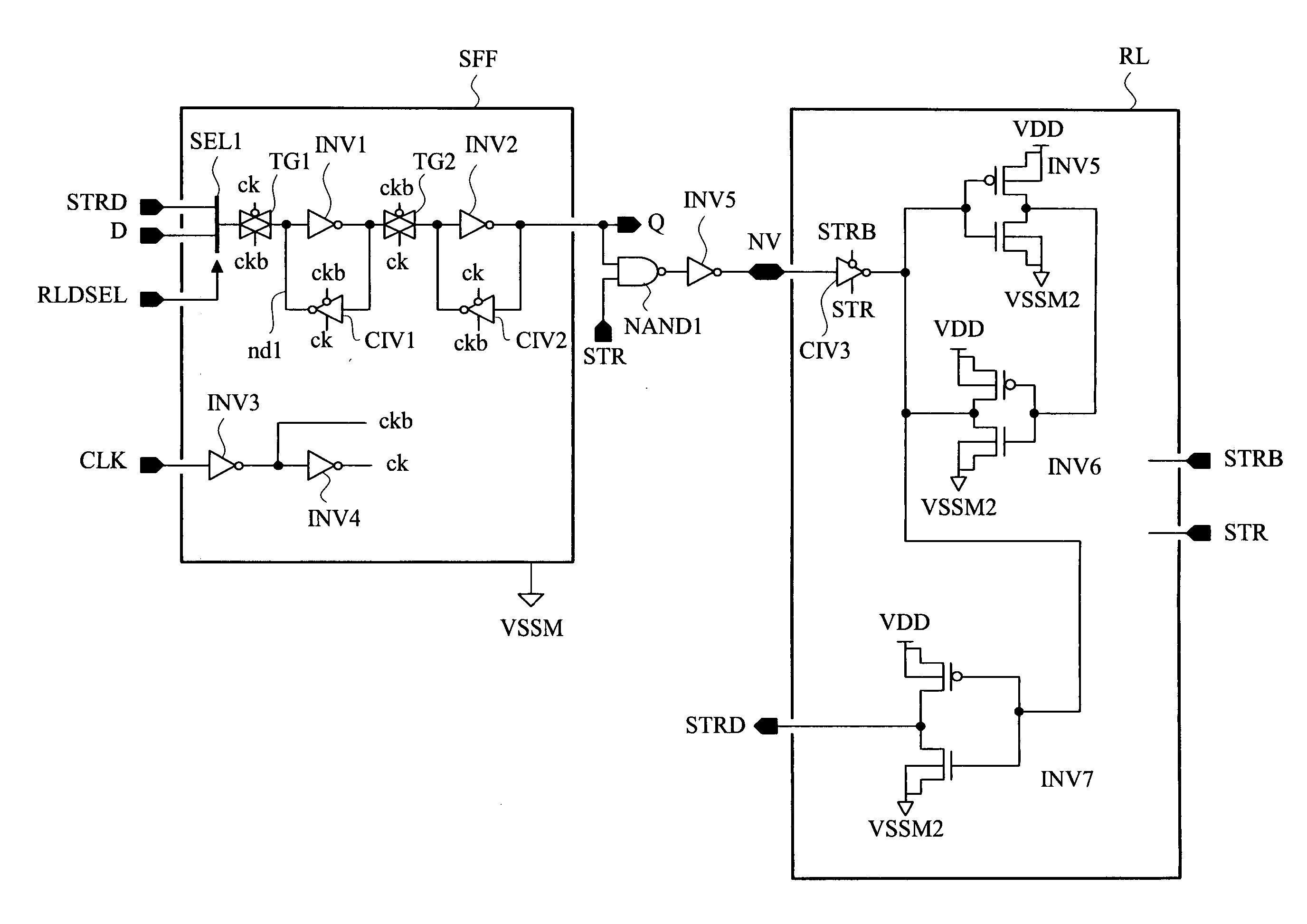
[0107]FIG. 8 shows an example of a layout of this subsidiary power domain. In FIG. 8, wirings extending in an x direction are provided with a first metal layer M1, and a VDD power supply VDD and a virtual ground power supply VSSM are wired. VSSM is provided as a power supply line that can be shut down from a true ground by means of a power switch described later. Hereinafter, while the present embodiment primarily describes a method for operating a circuit by using a virtual ground power supply VSSM and a VDD power supply VDD connected to a VSS power supply VSS via a switch, the present invention can be applied not only to power shutdown on such a VSS side but also to power shutdown on the VDD side similarly. In addition, the present invention can also be applied t...


PUM


Abstract

A semiconductor integrated circuit device is provided, the circuit being capable of arranging a control signal system, avoiding a danger of failure to check an indefinite signal propagation prevention circuit or the like, further facilitating a check oriented to mounting on an automated tool, and facilitating power shutdown control inside of a chip. In the semiconductor integrated circuit device, power shutdown priorities are provided by independent power domains Area A to Area I. A rule is provided, the rule defining that, in the case where a circuit having a high priority is turned ON, a power domain having its lower priority cannot be turned OFF, thereby facilitating a designing method. In addition, areas capable of applying still another power supply are provided in the independent power areas Area A to Area I. In that area, a relay buffer (repeater) and a clock buffer or an information retaining latch for saving information are integrated. A layout may be provided in a direction vertical to a direction in which cells are arranged in a row direction for the purpose of dispersing a current of a light supply line.

Description

CROSS-REFERENCE TO RELATED APPLICATION [0001] The present application claims priority from Japanese patent application No. JP 2005-166714 filed on Jun. 7, 2005, the content of which is hereby incorporated by reference into this application. BACKGROUND OF THE INVENTION [0002] The present invention relates to a semiconductor integrated circuit device. In particular, the present invention relates to a technique effectively applied to a system LSI for a portable device or a microprocessor. [0003] In recent years, with high integration caused by a finer semiconductor manufacturing process, an SoC (System-on-a-Chip) has been generally known such that almost of a system is integrated on one LSI. On the other hand, with this finer process, a leakage current in each transistor has increased more and more, and a leakage current of the whole SoC chip has become very large in amount. Conventionally, this leakage current has been importantly thought in a so-called standby state. However, in the ...

Claims


Application Information

Patent Timeline
Patent Type & Authority Applications(United States)
IPC IPC(8): H02H7/00H10B10/00
CPCH01L27/0207H01L27/11898H03K3/0375H01L23/48H01L27/02H01L2924/0002H01L27/0203H01L27/00H01L2924/00H03K19/0008H03K19/00346H03K17/16H01L29/7835G06F30/39G06F30/392G06F2117/04H01L23/50H01L23/528G11C11/419H01L27/11807H01L2027/11881H03K3/0315
Inventor KANNO, YUSUKEMIZUNO, HIROYUKIYASU, YOSHIHIKOHIROSE, KENJIIRITA, TAKAHIRO
Owner RENESAS ELECTRONICS CORP
Learn More