Non-volatile memory device having page buffer for verifying pre-erase

a non-volatile memory and buffer technology, applied in the field of non-volatile memory devices, can solve the problems of inability to perform pre-erase verification operations, excessive cell deletion,

Inactive Publication Date: 2006-12-28
SK HYNIX INC
View PDF3 Cites 28 Cited by
  • Summary
  • Abstract
  • Description
  • Claims
  • Application Information

AI Technical Summary

Problems solved by technology

In the case where an erase operation is performed in the NAND flash memory device, there is a case where a cell is excessively erased due to an erasing speed, the...

Method used


Image

  • Non-volatile memory device having page buffer for verifying pre-erase
  • Non-volatile memory device having page buffer for verifying pre-erase
  • Non-volatile memory device having page buffer for verifying pre-erase

Examples


Embodiment Construction

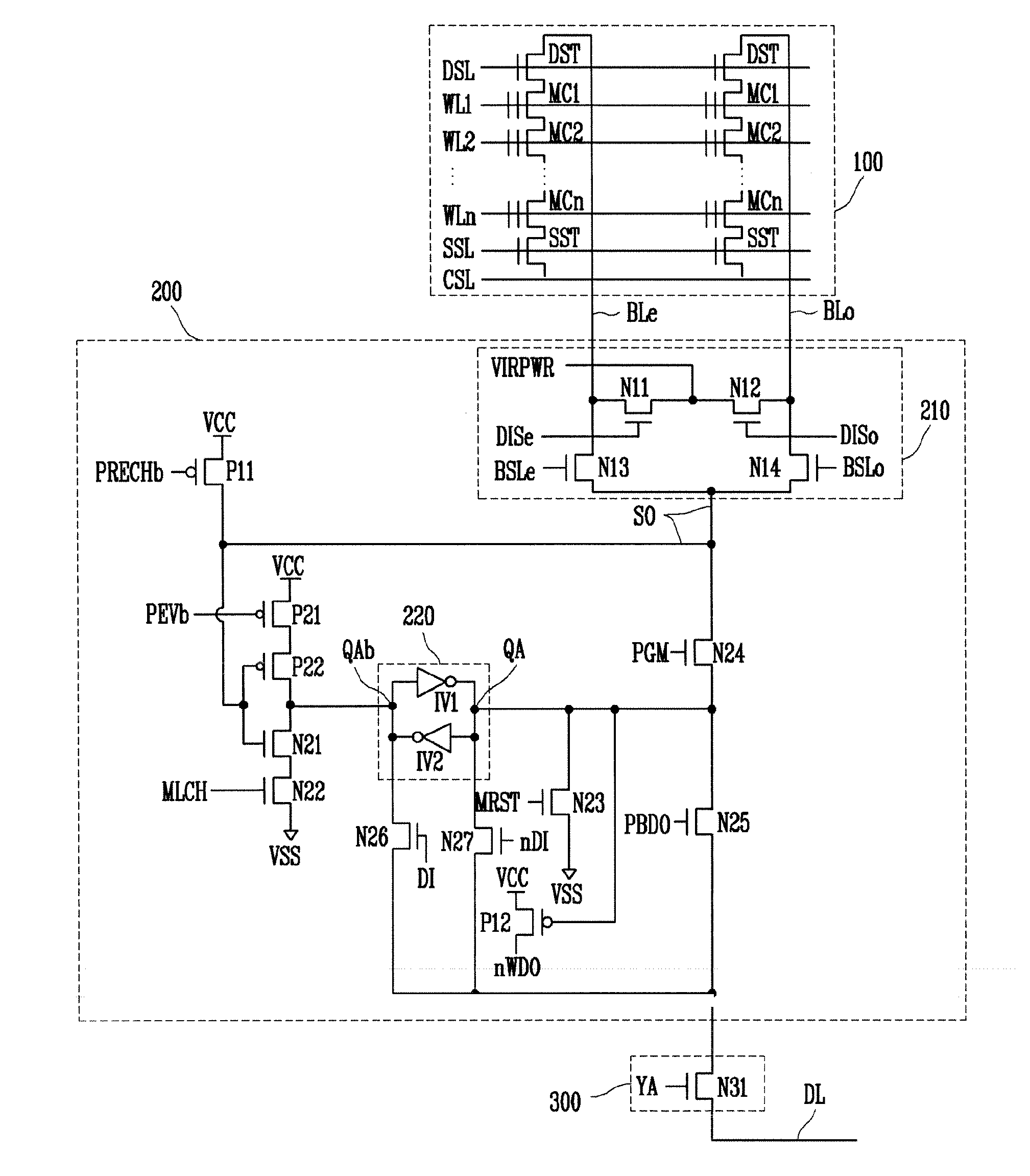
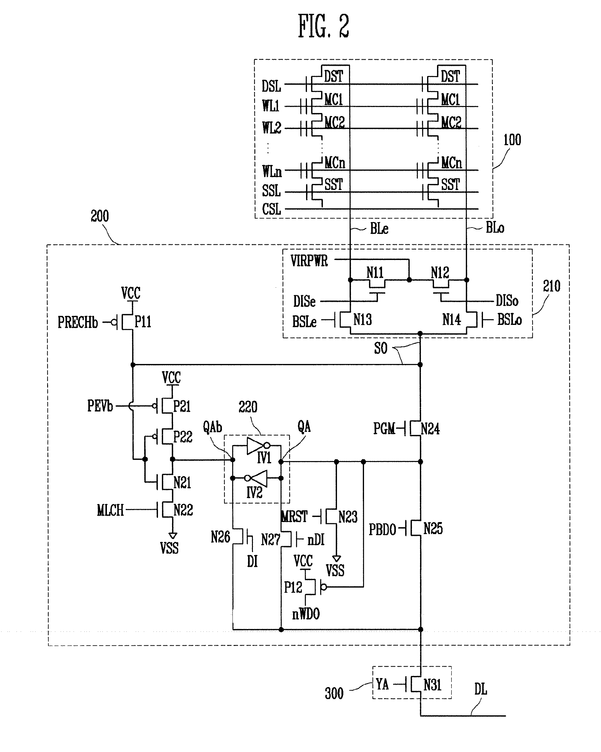
[0016]FIG. 2 is a circuit diagram of a NAND flash memory device that may have a page buffer for a pre-erase. The same reference numerals as those of FIG. 1 are used to identify the same or similar parts as those of FIG. 2.

[0017] Referring to FIG. 2, the NAND flash memory device may include a memory cell array 100, a page buffer 200 and a column select unit 300.

[0018] In the memory cell array 100, BLe indicates an even-numbered bit line, and BLo indicates an odd-numbered bit line. A plurality of memory cells MC1 to MCn is connected to the bit lines BLe, BLo, respectively, and is connected in series between a drain select transistor DST and a source select transistor SST to form one cell string. A memory cell (e.g., M1) is controlled by one word line (e.g., WL1) and forms one page.

[0019] A plurality of the page buffers 200 may include connected to the memory cell array 100. The plurality of page buffers performs a program, a read or an erase operation at the same time. In FIG. 2, o...


PUM


Abstract

Non-volatile memory devices have a page buffer that can verify pre-erase. A non-volatile memory device may include a cell array having a plurality of strings consisting of memory cells disposed at the intersection regions of bit lines and word lines, and a plurality of page buffers connected to the bit lines through a sensing line. Each of the plurality of page buffers may include a pre-erase detection unit that detects pre-erase in response to a signal of the sensing line in order to verify whether data programmed into the memory cells have been erased, a main erase detection unit that detects main erase in response to a signal of the sensing line in order to verify whether data programmed into the memory cells have been erased, a latch circuit which stores data in response to an output signal of the pre-erase detection unit at the time of pre-erase verify and stores data in response to an output signal of the main erase detection unit at the time of main erase verify, and a verify unit that verifies pass or fail of the pre-erase or main erase in response to a signal of the latch circuit at the time of pre-erase verify or main erase verify.

Description

TECHNICAL FIELD [0001] This patent relates to non-volatile memory devices, and more specifically, to a NAND flash memory device having a page buffer for pre-erase verification. DISCUSSION OF RELATED ART [0002] There is an increasing need for non-volatile memory devices which can be electrically programmed and erased and do not need for a refresh function of rewriting data at a constant cycle. The term “program” refers to an operation of writing data into memory cells. [0003] For higher integration of memory devices, a NAND flash memory device in which a plurality of memory cells is connected in series (i.e., a structure in which neighboring cells share the drain or source) to form one string has been developed. The NAND flash memory device is a memory device that sequentially reads information unlike a NOR flash memory device. [0004] The NAND flash memory device employs a page buffer in order to store a large capacity of information or read stored information with a short period of ...

Claims


Application Information

Patent Timeline
IPC IPC(8): G11C11/34
CPCG11C16/3454G02F1/1333G02F1/133331
Inventor LEE, JU YEAB
Owner SK HYNIX INC
Why Eureka
Try Eureka