Substrate cleaning brush, and substrate treatment apparatus and substrate treatment method using the same

Inactive Publication Date: 2007-01-11
SCREEN HLDG CO LTD
View PDF7 Cites 13 Cited by
  • Summary
  • Abstract
  • Description
  • Claims
  • Application Information

AI Technical Summary

Benefits of technology

[0017] The peripheral surface cleaning surface may be generally cylindrical. With this arrangement, the marginal portion of the substrate is cleaned by pressing the cylindrical peripheral surface cleaning surface against the peripheral surface of the substrate and pressing the marginal area cleaning su

Problems solved by technology

This necessitates replacement of the cleaning brush, inevitably lowering the productivity.
Therefore, it is impossi

Method used


Image

  • Substrate cleaning brush, and substrate treatment apparatus and substrate treatment method using the same
  • Substrate cleaning brush, and substrate treatment apparatus and substrate treatment method using the same
  • Substrate cleaning brush, and substrate treatment apparatus and substrate treatment method using the same

Examples


Example

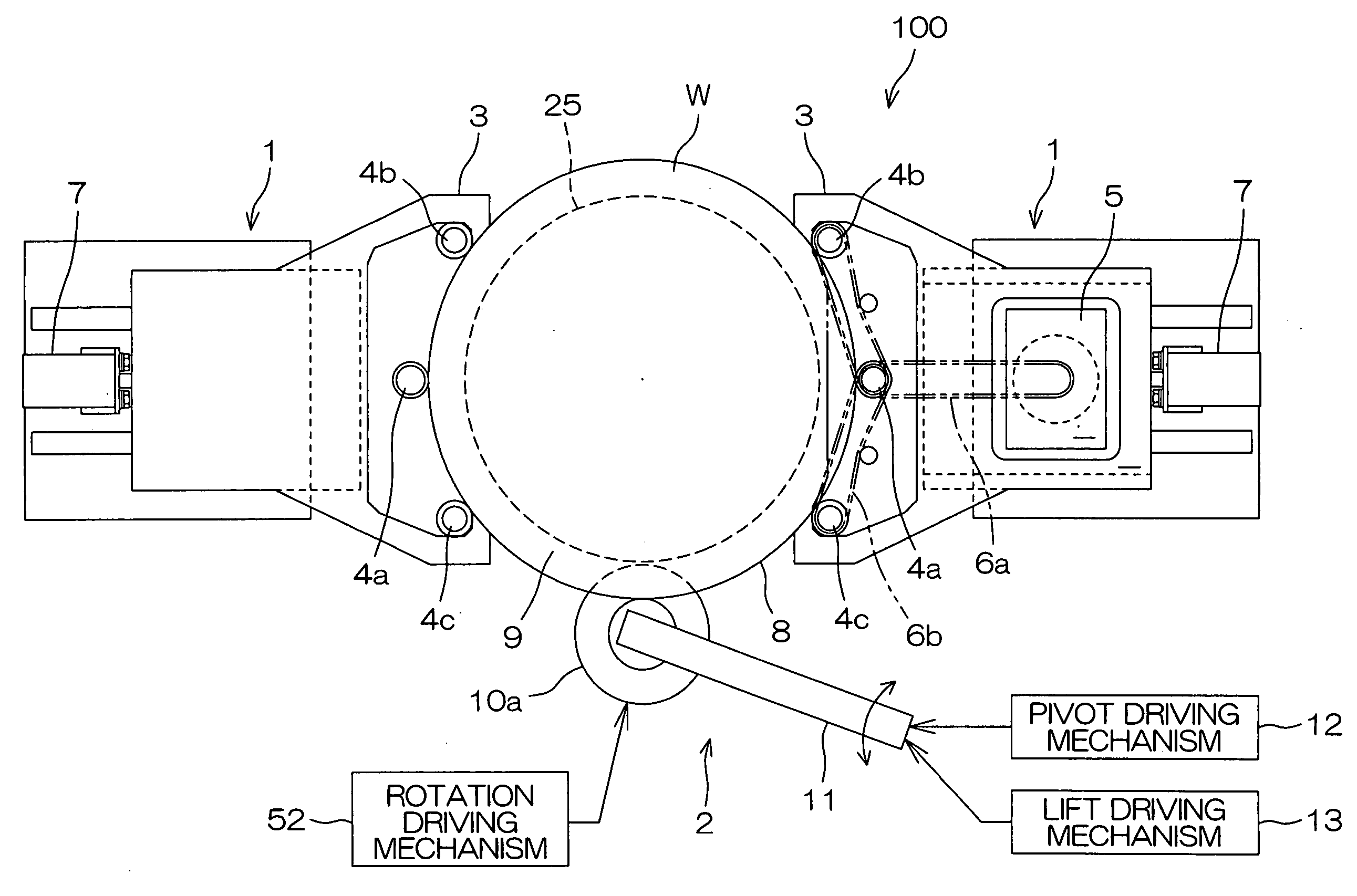
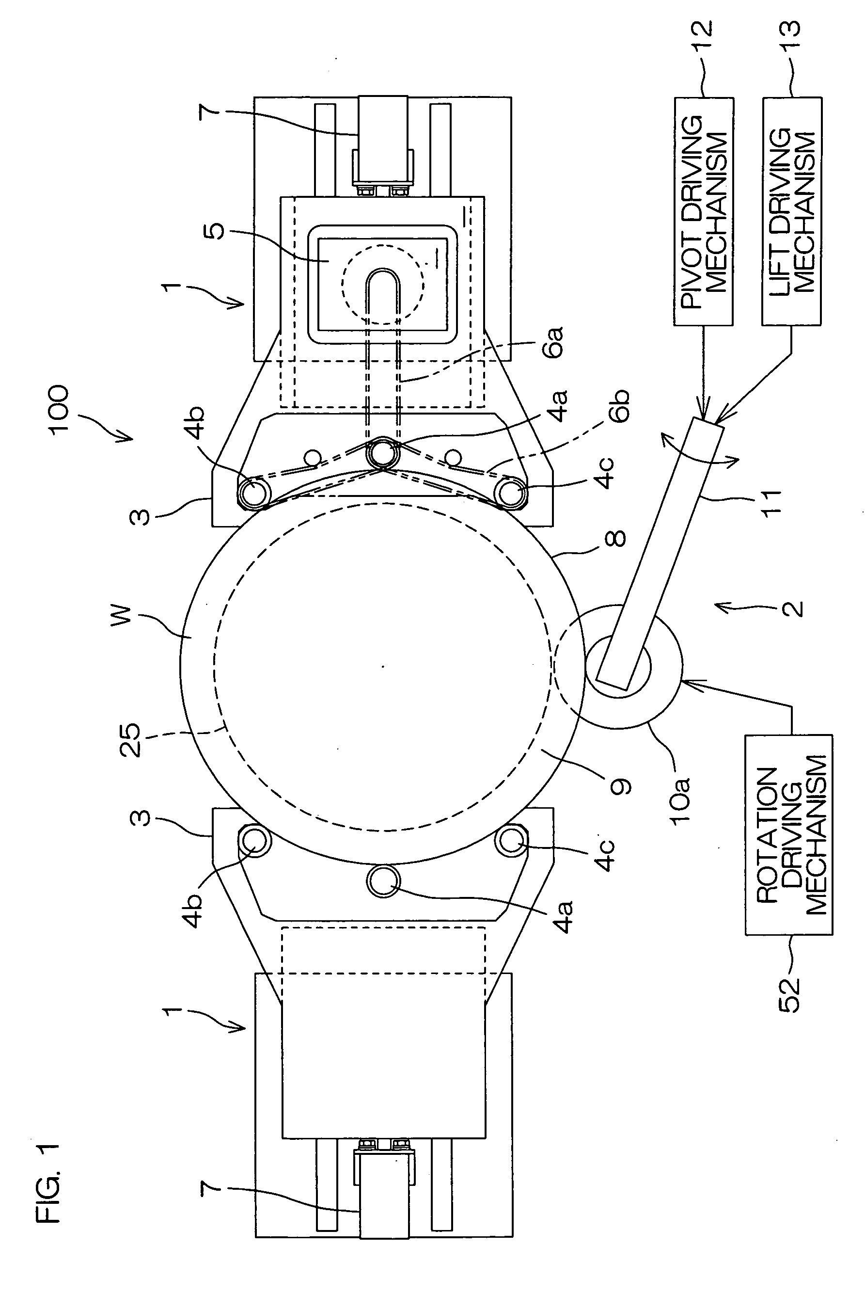
[0040]FIG. 1 is a plan view schematically illustrating the construction of a major portion of a substrate treatment apparatus according to one embodiment of the present invention. The substrate treatment apparatus 100 is of a single substrate treatment type, which is adapted to treat generally round substrates W (e.g., semiconductor wafers) on a one-by-one basis. The substrate treatment apparatus 100 includes a substrate holding / rotating mechanism 1 (serving as a substrate holding mechanism and a relative movement mechanism) which holds and rotates a substrate W, and a substrate cleaning mechanism 2 which scrubs the substrate W.

[0041] The substrate holding / rotating mechanism 1 has a pair of holder hands 3 disposed in opposed relation. The holder hands 3 each have three holder rollers 4a, 4b, 4c provided upright for holding the substrate W. The holder rollers 4a, 4b, 4c are arranged circularly in association with a peripheral surface of the substrate W. The substrate W is held horiz...


PUM


Abstract

An inventive substrate cleaning brush includes a peripheral surface cleaning portion, and a marginal area cleaning portion connected to the peripheral surface cleaning portion. The peripheral surface cleaning portion has a peripheral surface cleaning surface to be pressed against a peripheral surface of a substrate. The marginal area cleaning portion has a marginal area cleaning surface to be pressed against a marginal area of a major surface of the substrate, and the marginal area cleaning surface projects from the peripheral surface cleaning surface by a variable projection length.

Description

BACKGROUND OF THE INVENTION [0001] 1. Field of the Invention [0002] The present invention relates to a substrate cleaning brush, and a substrate treatment apparatus and a substrate treatment method using the substrate cleaning brush. Exemplary substrates to be treated with the use of the substrate cleaning brush include semiconductor wafers, substrates for liquid crystal display devices, substrates for plasma display devices, substrates for field emission display (FED) devices, optical disks and magnetic disks. [0003] 2. Description of Related Art [0004] In general, a surface of a semiconductor substrate (wafer) is not entirely used for device formation. That is, a marginal area of the surface of the semiconductor substrate having a predetermined width is a device non-formation region in which no device is formed. A center area of the surface of the semiconductor substrate inward of the device non-formation region serves as a device formation region. [0005] In a semiconductor device...

Claims


Application Information

Patent Timeline
IPC IPC(8): B08B7/00
CPCH01L21/67046B08B1/04H01L21/304
Inventor IWAMI, MASAKISATO, MASANOBU
Owner SCREEN HLDG CO LTD
Why Eureka
Try Eureka