Chip-embedded interposer structure and fabrication method thereof, wafer level stack structure and resultant package structure

a technology of chip-embedded interposers and stack structures, applied in the direction of semiconductor devices, semiconductor/solid-state device details, electrical apparatus, etc., can solve the problems of increasing the size of the stack structure, reducing the performance of the system, and increasing the cost of the product, so as to improve the interconnection efficiency and reduce the cost. the effect of the package size, the effect of improving the system performan

Inactive Publication Date: 2007-01-11
SAMSUNG ELECTRONICS CO LTD
View PDF20 Cites 87 Cited by
  • Summary
  • Abstract
  • Description
  • Claims
  • Application Information

AI Technical Summary

Benefits of technology

[0013] Another example embodiment of the present invention provides a system-in-package (SIP) having improved system performance, improved chip interconnections, and reduced package size.

Problems solved by technology

The use of the bonding wires 13 and the bumps 14 may result in relatively long connections, and possibly limitations of system performance and increased package size.
If the larger chip 22b is to be stacked on the smaller chip 22c, for example, the SIP 20 may have an impractical or overly complex stack structure.
Because the conventional SIPs 10 and 20 have different kinds of chips and of different sizes, a wafer level stack technique may be difficult to apply to the SIPs 10 and 20.

Method used


Image

  • Chip-embedded interposer structure and fabrication method thereof, wafer level stack structure and resultant package structure
  • Chip-embedded interposer structure and fabrication method thereof, wafer level stack structure and resultant package structure
  • Chip-embedded interposer structure and fabrication method thereof, wafer level stack structure and resultant package structure

Examples


Embodiment Construction

[0033] Example, non-limiting embodiments of the present invention will now be described more fully hereinafter with reference to the accompanying drawings. This invention may, however, be embodied in many different forms and should not be construed as limited to the particular example embodiments set forth herein. Rather, the disclosed embodiments establish a thorough and complete disclosure, and will convey the invention to those skilled in the art. The principles and feature of the present invention may be employed, therefore, in varied and numerous embodiments without departing from the scope of the invention.

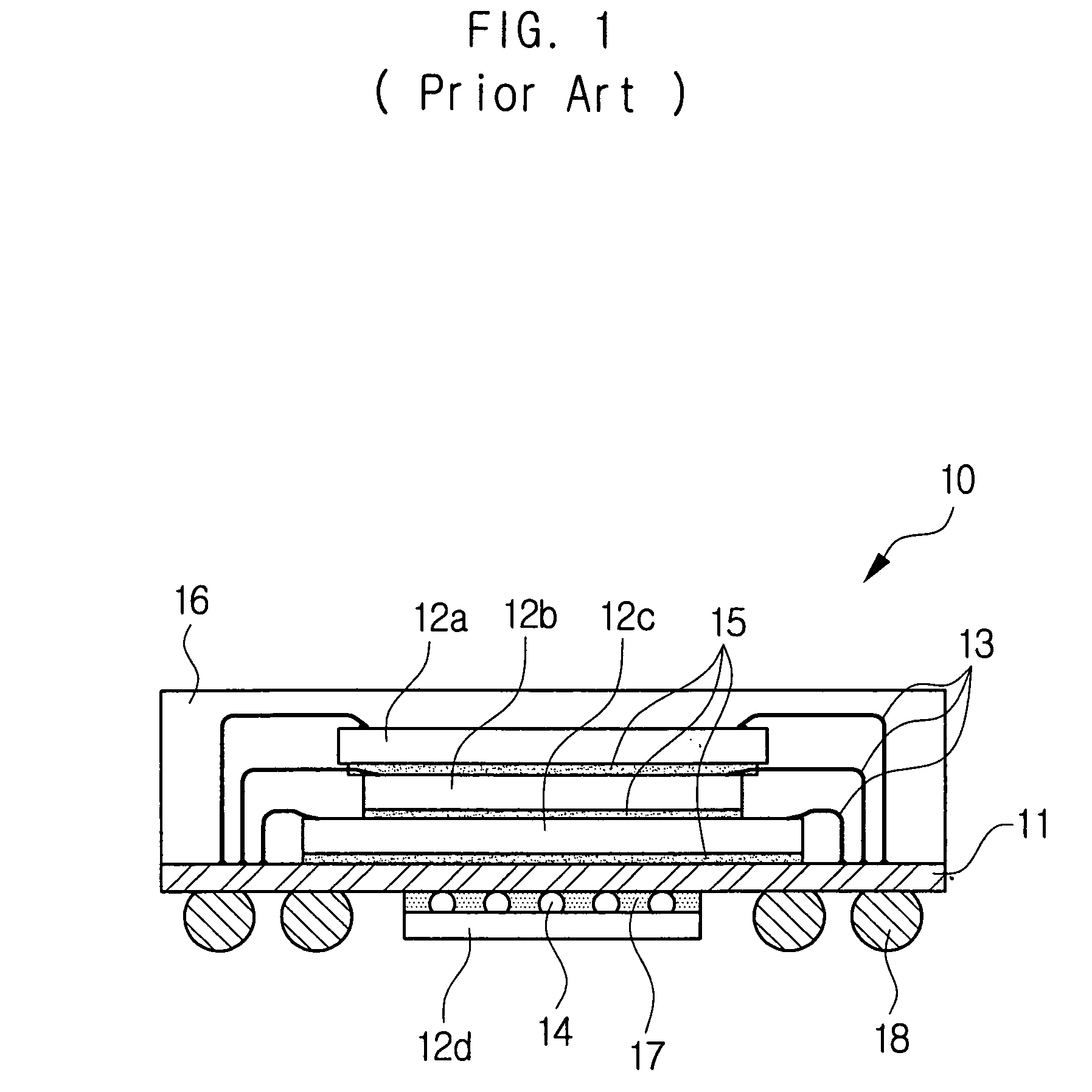
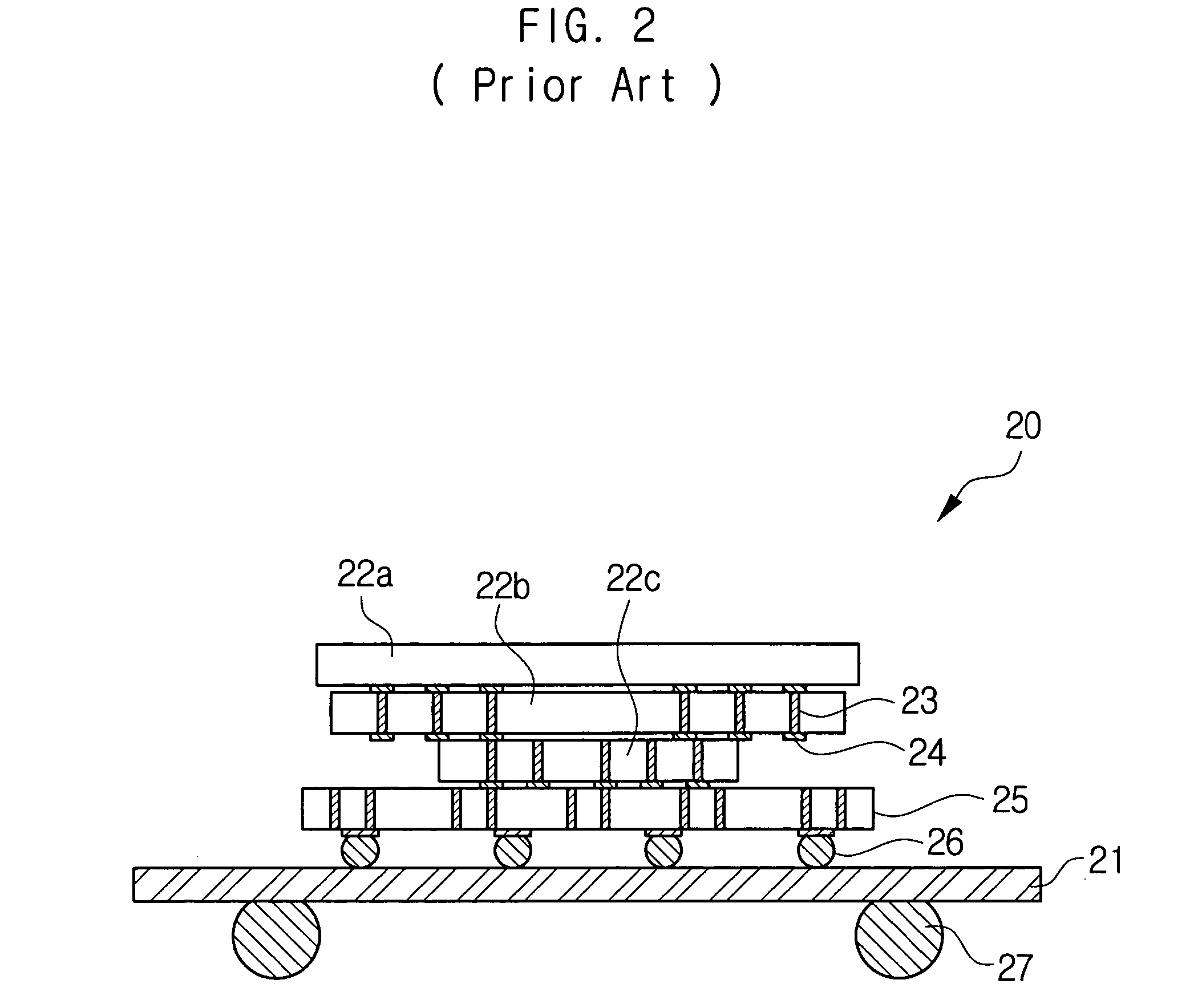
[0034] Well-known structures and processes are not described or illustrated in detail to avoid obscuring embodiments of the present invention. Like reference numerals are used for like and corresponding parts of the various drawings.

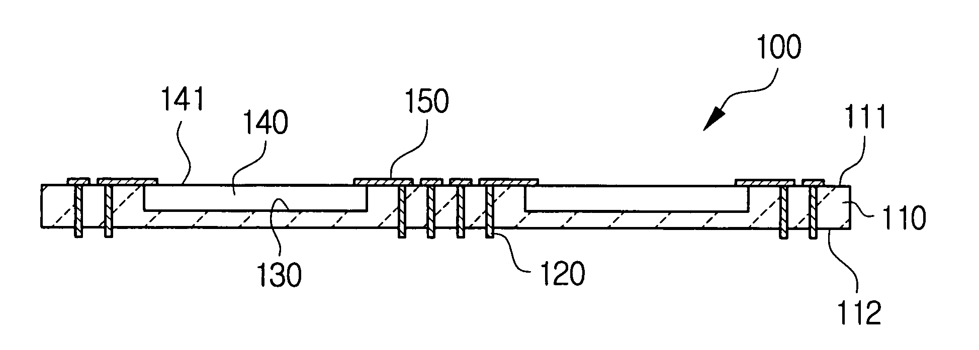
[0035]FIGS. 3A through 3F are cross-sectional views of a chip-embedded interposer 100 and a related fabrication method in accordance with an e...


PUM


Abstract

A method for fabricating a chip-embedded interposer may comprise forming at least one cavity on a silicon substrate, forming a plurality of through vias penetrating the silicon substrate, providing an integrated circuit chip having a plurality of I/O pads, and forming rerouting conductors connected to the I/O pads and the through vias. A stack structure having different kinds of chips may be incorporated at wafer level using the described interposer.

Description

CROSS REFERENCE TO RELATED APPLICATIONS [0001] This U.S. non-provisional application claims benefit of priority under 35 U.S.C. § 119 of Korean Patent Application No. 2005-61573, filed on Jul. 8, 2005, the entire contents of which are incorporated herein by reference.BACKGROUND OF THE INVENTION [0002] 1. Field of the Invention [0003] The present invention relates to a semiconductor packaging structure and technique and, more particularly, to a structure and technique for stacking different kinds of integrated circuit chips regardless of chip size. [0004] 2. Description of the Related Art [0005] With the advent of a digital network information age, electronic products have been developing rapidly. For example, multimedia products, digital electrical household appliance products and personal digital products are developing rapidly and will likely continue to do so. Under such rapid development, the electronic industry must manufacture reliable, light, compact, high-speed, multifunctio...

Claims


Application Information

Patent Timeline
Patent Type & Authority Applications(United States)
IPC IPC(8): H01L23/52
CPCH01L23/5389H01L2224/0401H01L25/0657H01L2224/16H01L2224/32145H01L2224/73265H01L2224/97H01L2225/0652H01L2225/06541H01L2225/06551H01L2225/06572H01L2225/06586H01L2924/01015H01L2924/01029H01L2924/01074H01L2924/01075H01L2924/01078H01L2924/01079H01L2924/01082H01L2924/14H01L2924/15311H01L2924/1532H01L2924/30105H01L24/97H01L2924/157H01L2924/15153H01L2224/73267H01L2224/24226H01L24/82H01L24/24H01L2924/01005H01L2924/01006H01L2924/01033H01L2924/01076H01L2224/48227H01L2224/04105H01L2224/24227H01L2224/32225H01L2924/00H01L2224/83H01L2224/82H01L2924/181H01L2224/83192H01L2224/92244H01L2924/00012H01L23/12
Inventor LEE, KANG-WOOKKIM, GU-SUNGKWON, YONG-CHAIMA, KEUM-HEEHAN, SEONG-IL
Owner SAMSUNG ELECTRONICS CO LTD
Why Eureka
Try Eureka