Method for sensor edge and mask height control for narrow track width devices

Inactive Publication Date: 2007-01-11
WESTERN DIGITAL TECH INC
View PDF6 Cites 3 Cited by
  • Summary
  • Abstract
  • Description
  • Claims
  • Application Information

AI Technical Summary

Benefits of technology

[0009] One embodiment of a system, method, and apparatus for obtaining well-defined DLC mask edges is to have a static mask for the DLC layer. In the solution of the present invention, a RIE-resistant and/or CMP-resistant layer is deposited after the DLC layer. This new layer can be relatively thin since th

Problems solved by technology

Current mask processes can be prone to track width (TW) control and junction definition issues between the various layers of the product that define the sensor width.
This makes it nearly impossible to obtain well-defined DLC edges, which can induce large junction variations.
Another problem is encountered during RIE processing of relatively narrow TW sensor structures.
Thus, narrow TW devices have less resist and therefore offer

Method used


Image

  • Method for sensor edge and mask height control for narrow track width devices
  • Method for sensor edge and mask height control for narrow track width devices
  • Method for sensor edge and mask height control for narrow track width devices

Examples


Embodiment Construction

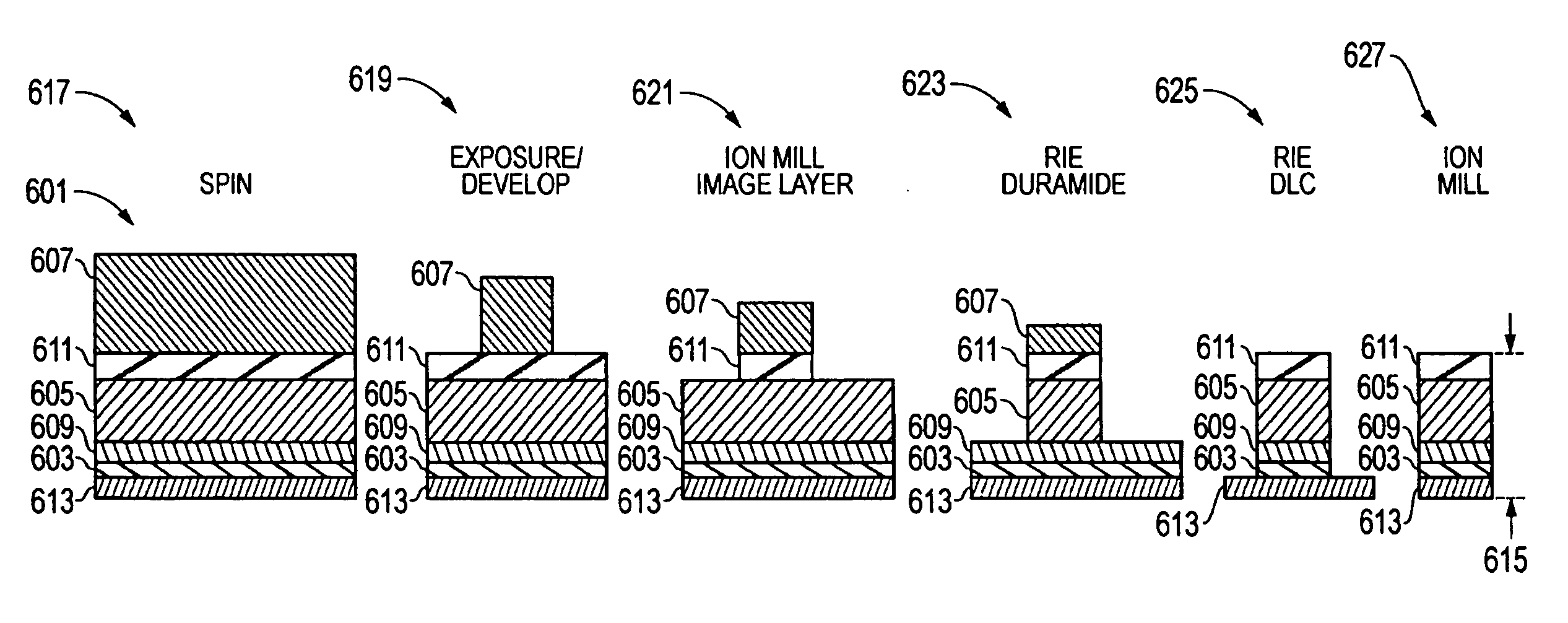
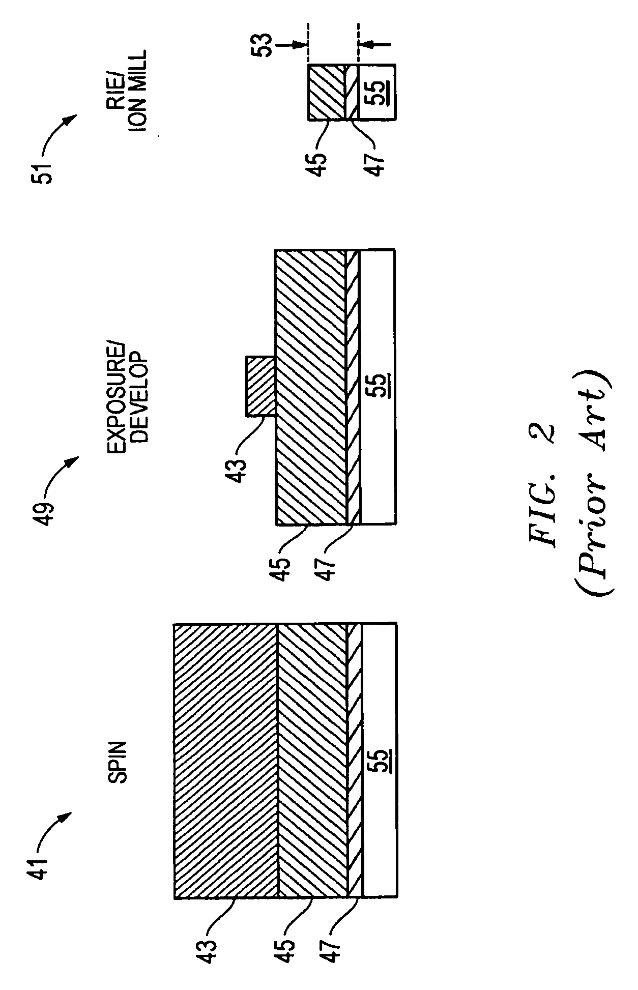
[0018] Referring to FIGS. 3 and 4, embodiments of the present invention are shown. At its most basic level, the present invention comprises a system and method of forming a mask for a structure.

[0019] In FIG. 3, the mask or image layer 509 is located directly between the duramide and TIS layers 505, 507. The image layer 509 is RIE-resistant and, in one embodiment, CMP resistant as well. In another embodiment (FIG. 4), the image layer comprises two different image layers 609 and 611. First image layer 609 is located directly between the DLC and duramide layers 603, 605, and second image layer 611 is located directly between the duramide and TIS layers 605, 607.

[0020] In the embodiments of FIGS. 3 and 4, the mask or image layers 509, 611, respectively, may be located directly between the duramide and TIS layers 505, 507 and 605, 607, respectively, in order to better control the mask height 515, 615 (far right side of FIGS. 3 and 4, respectively). The image layer(s) may be removed wi...


PUM


Abstract

A process for defining and controlling the mask height of sensor devices is disclosed. An RIE-resistant, image layer, such as Cu or NiFe, is deposited after the DLC layer. A combination of RIE and ion milling processes or reactive ion beam etching processes are used to form the mask structure. Having an RIE-resistant layer precisely defines the DLC edge and minimizes the line edge roughness that result from fast removal of duramide during RIE. This solution controls the formation of the edges of the sensors and provides good definition for DLC mask edges. The image layer may be chemical mechanical polished to eliminate ion milling before the final RIE step.

Description

BACKGROUND OF THE INVENTION [0001] 1. Technical Field [0002] The present invention relates in general to the masking of devices during processing and, in particular, to an improved system and method for masking of sensors during processing for better control of sensor edges and mask height for sensors having a narrow track width. [0003] 2. Description of the Related Art [0004] Current mask processes can be prone to track width (TW) control and junction definition issues between the various layers of the product that define the sensor width. These problems are illustrated in FIG. 1, which is a tunneling electron microscope (TEM) image of a sectioned masked wafer site 17. For example, the freelayer of the sensor has a TW length 11 that is wider than the width 13 of the mask. In addition, the side 15 of the mask (e.g., into and out of the page) is relatively rough rather than straight, and the edges of the diamond-like carbon (DLC) mask layer are sloped rather than relatively sharp. [0...

Claims


Application Information

Patent Timeline
IPC IPC(8): H01L21/00H01L21/302H01L21/461
CPCG11B5/3163G11B5/3116
Inventor PINARBASI, MUSTAFA MICHAEL
Owner WESTERN DIGITAL TECH INC
Why Eureka
Try Eureka