Element substrate, test method for element substrate, and manufacturing method for semiconductor device
- Summary
- Abstract
- Description
- Claims
- Application Information
AI Technical Summary
Benefits of technology
Problems solved by technology
Method used
Image

Examples
Example
Embodiment 1
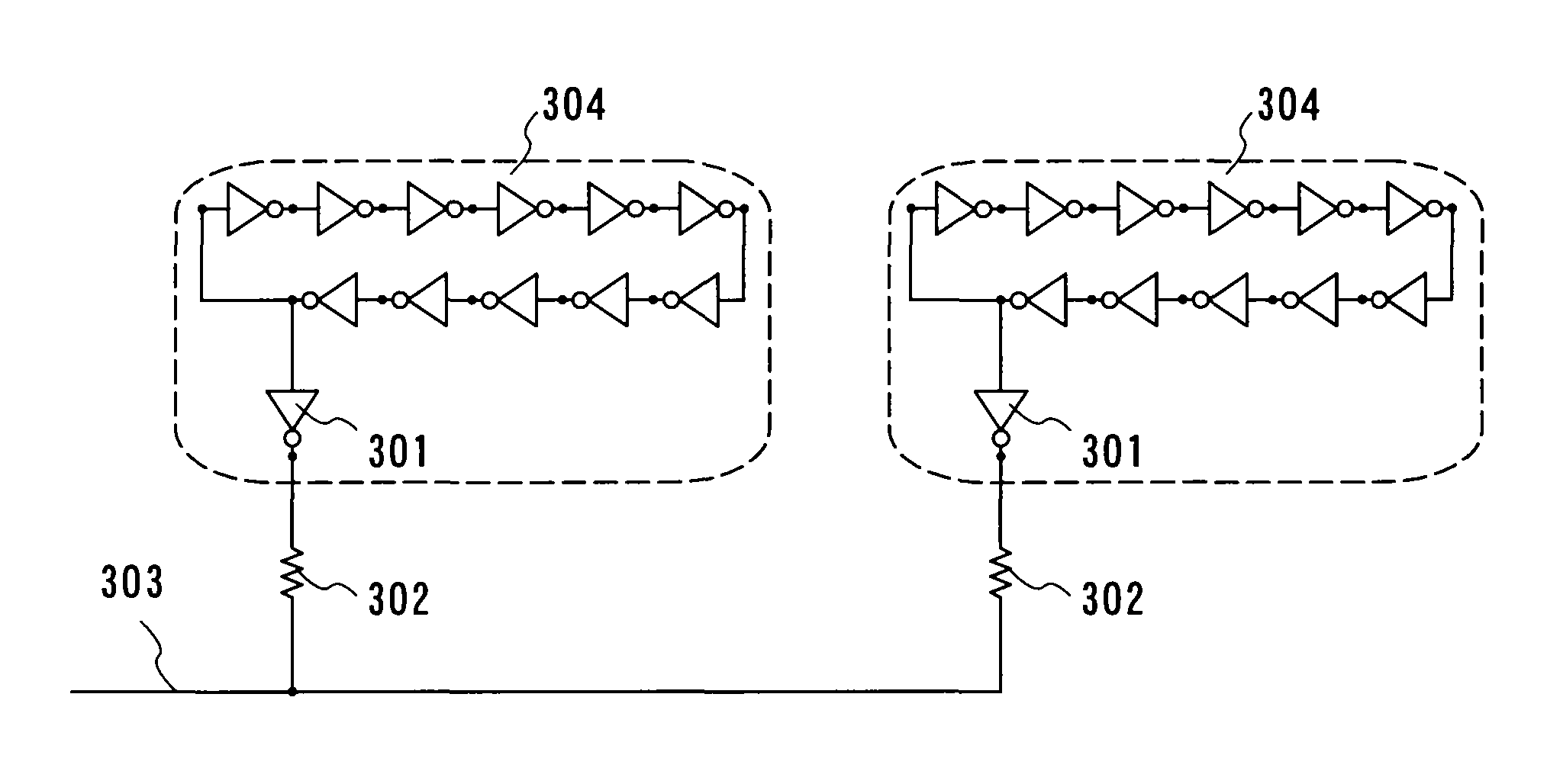
[0091] This embodiment shows a circuit diagram of an oscillation circuit for evaluation that is constituted by a ring oscillator. FIG. 3 corresponds to the structure shown in FIG. 2. In FIG. 3, two ring oscillators are connected through a resistor 302. In the invention, the oscillation circuit for evaluation is not limited to the ring oscillator, and may be a PLL, a VCO, or an LC oscillation circuit. This embodiment shows the case of the ring oscillator. In the invention, the number of oscillation circuits for evaluation may be two or more, and this embodiment shows the case where two ring oscillators are provided.
[0092] In FIG. 3, each of ring oscillators 304 is constituted by 11 inverter elements, and includes an inverter element as an output buffer 301. Note that the number of inverter elements constituting the ring oscillator is not limited to 11, and the ring oscillator may be constituted by an odd number of inverter elements. If a ring oscillator is constituted b...
Example
Embodiment 2
[0106] In this embodiment, manufacturing steps of a semiconductor device using the test method of the invention are described.
[0107] A base film is provided over an insulating substrate. Thin film transistors are formed over the insulating substrate with the base film interposed therebetween. The thin film transistors can be used as elements of a pixel portion or a driver circuit portion of the semiconductor device. Each of the thin film transistors includes an island shaped semiconductor film, and a gate electrode provided thereover with a gate insulating film interposed therebetween. It is preferable to provide an insulator (a so-called side wall) on each side surface of the gate electrode, so that the side wall can prevent short channel effects. The semiconductor film is formed to have a thickness of 0.2 μm or less, typically 40 to 170 nm, and preferably 50 to 150 nm. Further, the thin film transistor includes an insulating film covering the semiconductor film, and ...
Example
Embodiment 3
[0117] In this embodiment, a layout of a semiconductor device using the evaluation method of the invention is described.
[0118] In a thin film transistor of the invention, a photomask for forming a semiconductor layer has a pattern. This pattern of the photomask has a corner that is rounded by removing a right triangle with one side of 10 μm or shorter in a corner portion. The shape of this mask pattern can be transferred as a pattern of a semiconductor layer 1000 as shown in FIG. 10. The mask pattern may be transferred to the semiconductor layer so that the corner of the semiconductor layer is more rounded than the corner of the mask pattern. In other words, the semiconductor layer may have a pattern with a corner that is more rounded than the corner of the mask pattern. Note that in FIG. 10, gate electrodes and wires formed later are denoted by dotted lines.
[0119] Then, a gate insulating film is formed over the semiconductor layer processed to have a rounded corner. ...
PUM
 Abstract
Description
Claims
Application Information
 - R&D Engineer
- R&D Manager
- IP Professional
- Industry Leading Data Capabilities
- Powerful AI technology
- Patent DNA Extraction
Browse by: Latest US Patents, China's latest patents, Technical Efficacy Thesaurus, Application Domain, Technology Topic.
© 2024 PatSnap. All rights reserved.Legal|Privacy policy|Modern Slavery Act Transparency Statement|Sitemap