Optimized photomasks for photolithography

a photolithography and photolithography technology, applied in the field of masks, can solve problems such as sub-optimal designs, patterns may not print correctly at all, and unwanted distortions and artifacts accompanied by

Inactive Publication Date: 2007-01-11
DINO TECH ACQUISITION
View PDF44 Cites 31 Cited by
  • Summary
  • Abstract
  • Description
  • Claims
  • Application Information

AI Technical Summary

Benefits of technology

[0007] Optimization utilizes “merit function” for encoding aspects of photolithographic process, preferences relating to resulting pattern (e.g. restriction to

Problems solved by technology

However, due to the wave nature of light, as dimensions approach sizes comparable to the wavelength of the light used in the photolithography process, the resulting wafer patterns deviate from the corresponding photomask patterns and are accompanied by

Method used


Image

  • Optimized photomasks for photolithography
  • Optimized photomasks for photolithography
  • Optimized photomasks for photolithography

Examples


Embodiment Construction

)

[0028] As understood herein, the term “wafer pattern” is understood to include any polygon (rectilinear or non-rectilinear) or other shape or pattern to be formed on a semiconductor or other material substrate, for example digital or analog circuit structures or interconnect.

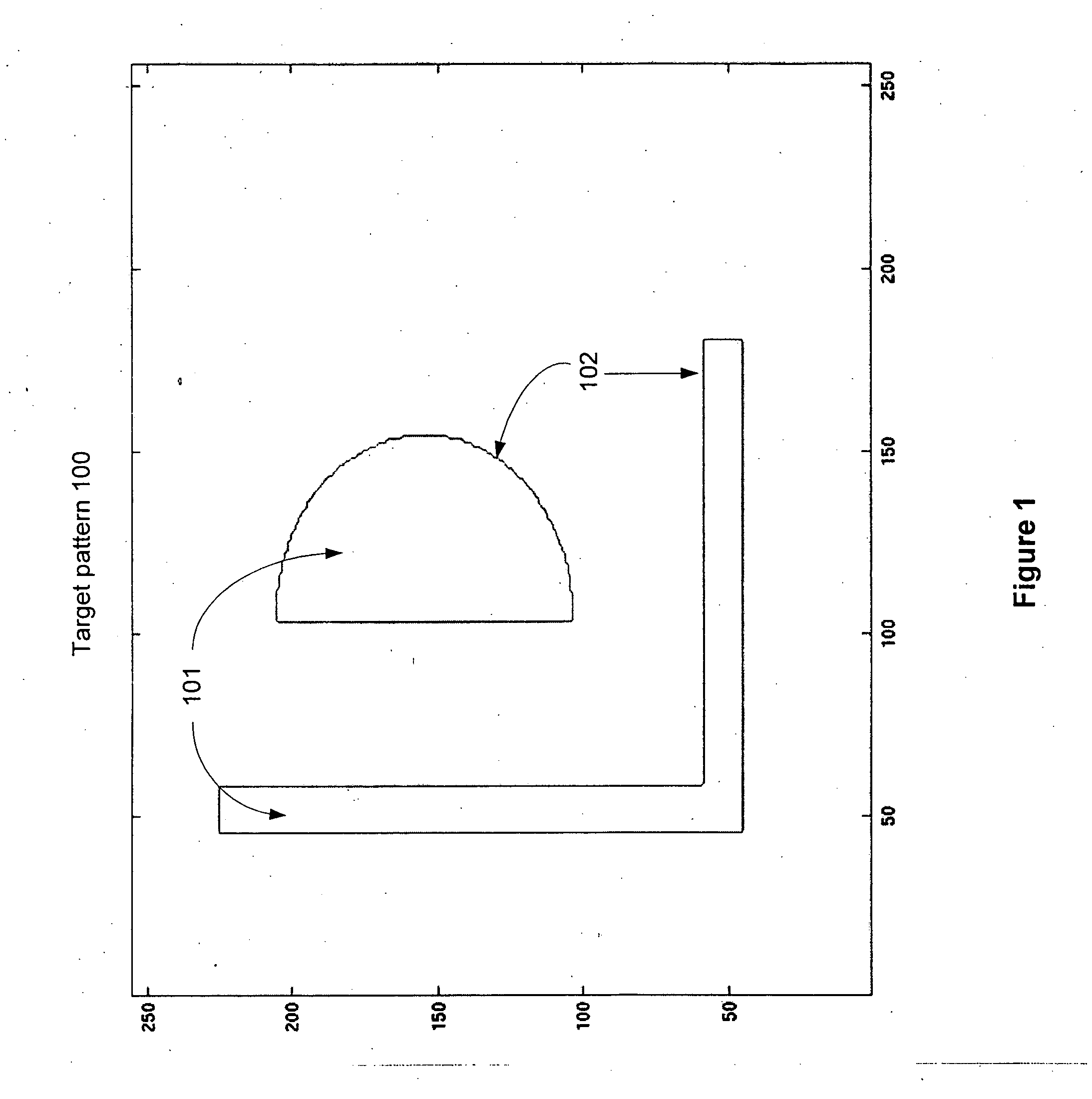
[0029]FIG. 1 is a diagram illustrating an example target pattern 100 to be printed on a wafer using a photolithography process. Target pattern 100 comprises regions 101 enclosed by contours 102. Preferably, areas within regions 101 represent photoresist and the area outside regions 101 represents the absence of photoresist.

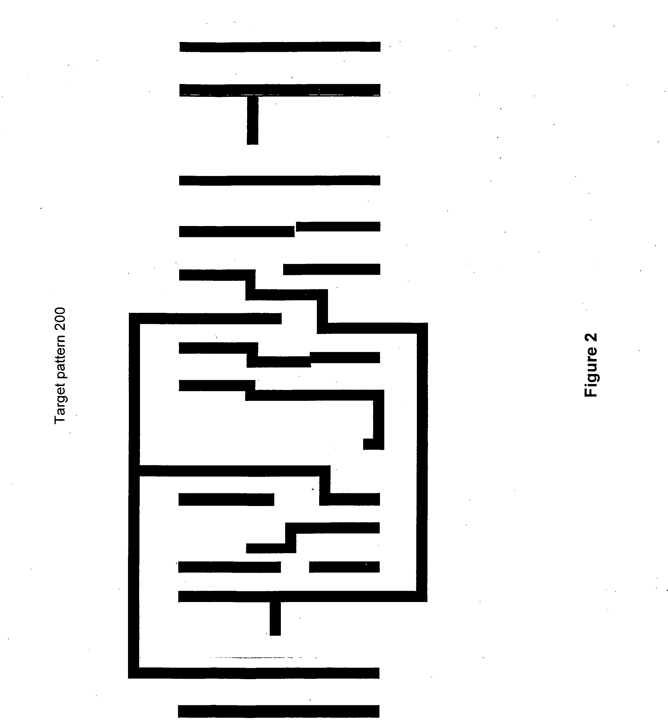
[0030]FIG. 2 is a diagram illustrating a more complex example target pattern 200 to be printed on a wafer using a photolithography process. The complexity of target pattern 200 is more illustrative of a pattern for representing an integrated circuit design.

[0031]FIG. 3 is a diagram illustrating a detail target pattern 300 from the example target pattern 200 of FIG. 2 to be printed on a waf...


PUM


Abstract

Photomask patterns are represented using contours defined by level-set functions. Given target pattern, contours are optimized such that defined photomask, when used in photolithographic process, prints wafer pattern faithful to target pattern. Optimization utilizes “merit function” for encoding aspects of photolithographic process, preferences relating to resulting pattern (e.g. restriction to rectilinear patterns), robustness against process variations, as well as restrictions imposed relating to practical and economic manufacturability of photomasks.

Description

CROSS-REFERENCE [0001] This application is a continuation application of Application Ser. No. 10 / 408,924, filed Apr. 6, 2003, which is incorporated herein by reference in its entirety and to which application we claim priority under 35 USC §120.FIELD OF INVENTION [0002] Invention relates to masks, also known as photomasks, used in photolithography processes and, more particularly, to a method for applying level-set technology to time-evolve contours representing patterns on photomasks in such a way so as to allow for production of wafer patterns with minimal distortions or artifacts and to allow for the ability to constrain resulting contours to rectilinear patterns. DESCRIPTION OF RELATED ART [0003] Lithography processing represents an essential technology for manufacturing Integrated Circuits (IC) and Micro Electro-Mechanical Systems (MEMS). Lithographic techniques are used to define patterns, geometries, features, shapes, et al (“patterns”) onto an integrated circuit die or semic...

Claims


Application Information

Patent Timeline
IPC IPC(8): G06F17/50
CPCG03F1/144G06F2217/12G06F17/5068G03F1/36G06F30/39G06F2119/18Y02P90/02
Inventor ABRAMS, DANIELPENG, DANPINGOSHER, STANLEY
Owner DINO TECH ACQUISITION
Why Eureka
Try Eureka