Electroluminescence display device

a display device and electroluminescent technology, applied in static indicating devices, electroluminescent light sources, instruments, etc., can solve the problems of limiting the reduction of the width of the frame portion, reduce the number of lines and terminals, reduce the influence of voltage drop, and reduce the number of terminals.

Active Publication Date: 2007-01-18
SANYO ELECTRIC CO LTD
View PDF11 Cites 15 Cited by
  • Summary
  • Abstract
  • Description
  • Claims
  • Application Information

AI Technical Summary

Benefits of technology

[0036] By connecting the power supply line for the horizontal scan driver circuit and the power supply line for the vertical scan driver circuit to a common external connection terminal and branching the line to connect one of the branches to the horizontal scan driver circuit and the other of the branches to the vertical scan driver circuit, it is possible to reduce the number of lines and terminals up to the point of branching. In addition, by branching the lines, it is possible to reduce the influences of the voltage drop in one of the driver circuits on the other driver circuit.
[0037] By providing he vertical scan driver circuit on a second side which opposes the first side on which the external connection terminal is provided, it is possible to place the horizontal scan driver circuit on a third side which is in contact with the vertical scan driver circuit. In this manner, the line distance to the driver circuits can be easily minimized. Furthermore, it is not necessary to provide a power supply line or the like for the driver circuit on a fourth side opposing the third side on which the horizontal scan driver circuit is placed. Thus, a drive line portion for supplying the driving power to the electroluminescence element can be formed with a wide width on the fourth side and the variation or the like of light emission brightness of the electroluminescence elements on a display screen due to the voltage drop in the drive line portion can be reliably reduced.
[0038] Because it is not necessary to place either a driver circuit or drive line portion for the electroluminescence element on the first side, it is possible to place, on the first side, a contact region between the common electrode of the electroluminescence elements of the pixels and the common electrode line extending from the external connection terminal corresponding to the common electrode, and, thus, the size of the contact region can easily be maximized to reduce the line resistance.
[0039] By placing, among the external connection terminals, the terminal for horizontal scan-related line, terminal for the cathode power supply, and the terminal for pixel driving power supply in this order from an upper side toward the lower side, it is possible to reduce the length of the line without significantly changing the conventional layout. By reducing the line length, it is possible to inhibit power loss in this portion.
[0040] By placing the terminal for the pixel driving power supply at a position lower than a center line extending along a horizontal direction of the display region of the display device, it is possible to shorten the length of the line through which the drive current flows, and, thus reduce the line load such as the line resistance. In this manner, it is possible to inhibit the power loss in these portions.
[0041] By placing the vertical scan driver circuit of the display device adjacent to a lateral side opposing the lateral side on which the external connection terminal is provided, it is possible to efficiently use the region at the periphery of the display region for sealing the organic EL element. In other words, the vertical scan driver circuit is placed below the region for sealing to effectively use the space. This configuration is advantageous in narrowing the width of the frame portion, that is, a region between the display region and the edge of the panel substrate, in equating or approximately equating the width of the frame portions, reducing the deviation of origins of the panel substrate and the display region, and reducing the outer size of the panel substrate.

Problems solved by technology

In addition, because the width of the frame portion of the lower side is larger compared to those of the other sides, there is a constraint in the layout when such a display panel is integrated into various devices as a display device.
However, in these devices also, a line for supplying power must extend into a portion of the lower side, limiting reduction of the width of the frame portion.

Method used


Image

  • Electroluminescence display device
  • Electroluminescence display device
  • Electroluminescence display device

Examples


Embodiment Construction

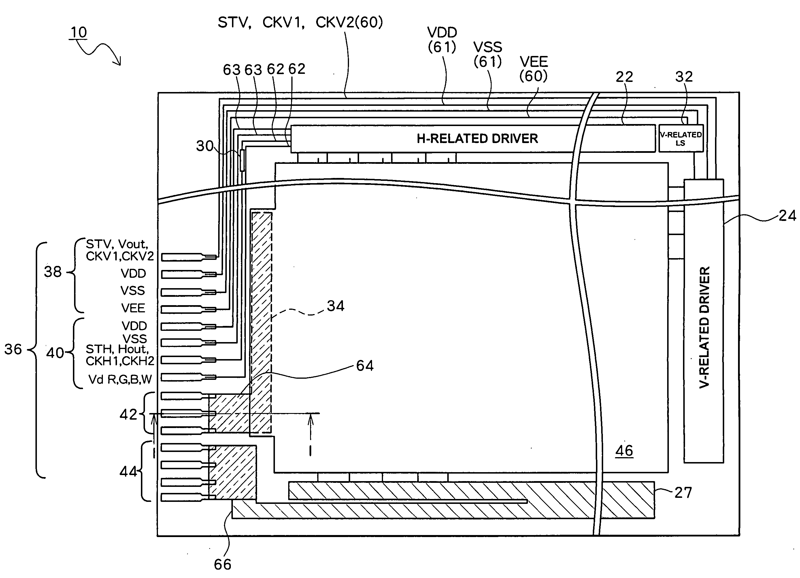
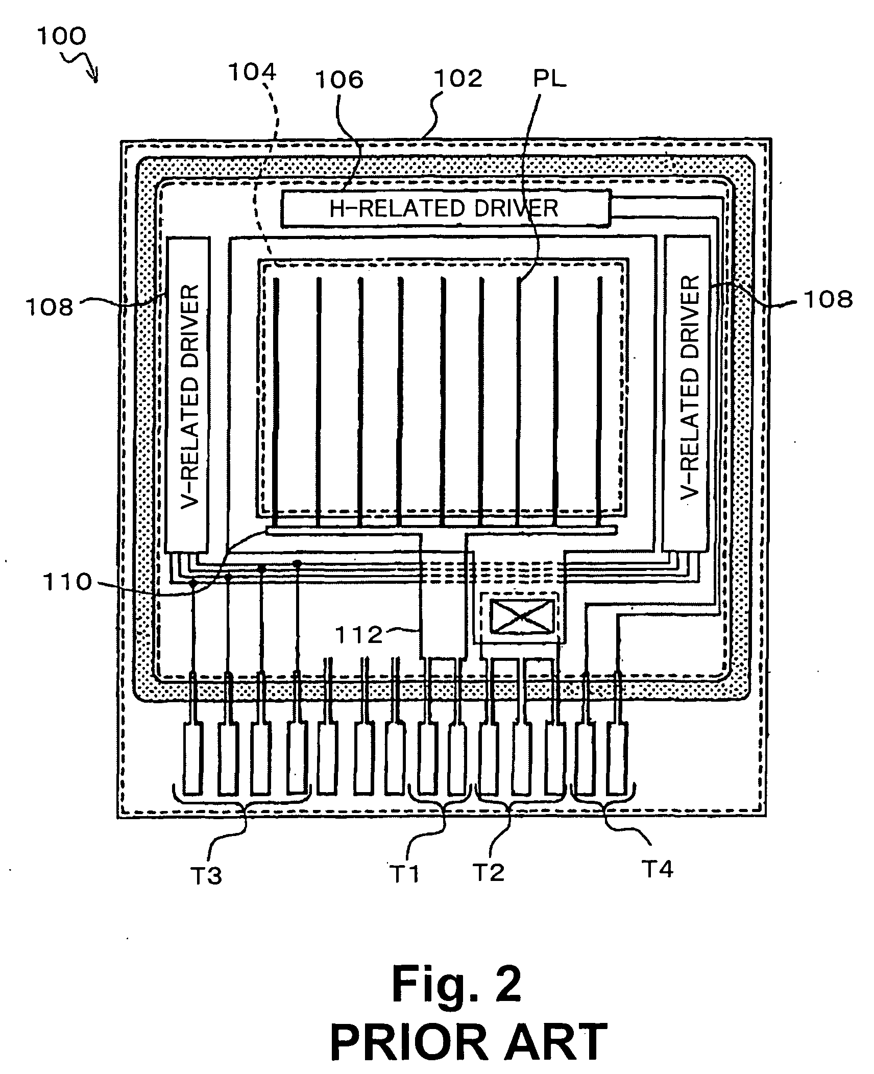
[0053] Preferred embodiments of the present invention will now be described referring to the drawings. FIG. 3 is a diagram schematically showing a placement of an EL display panel 10 according to a preferred embodiment of the present invention. A display region (display portion) 14 is formed on a panel substrate 12 with a plurality of pixels arranged in a matrix form. In the display region 14, a gate line 16 (GL) to which a selection signal is sequentially output is formed along a horizontal scan (row) direction of the matrix and a data line 18 (DL) to which a data signal is output and a power supply line 20 (PL) for supplying an operational power supply (PVDD) to an organic EL element which is an element to be driven are formed along a vertical scan (column) direction.

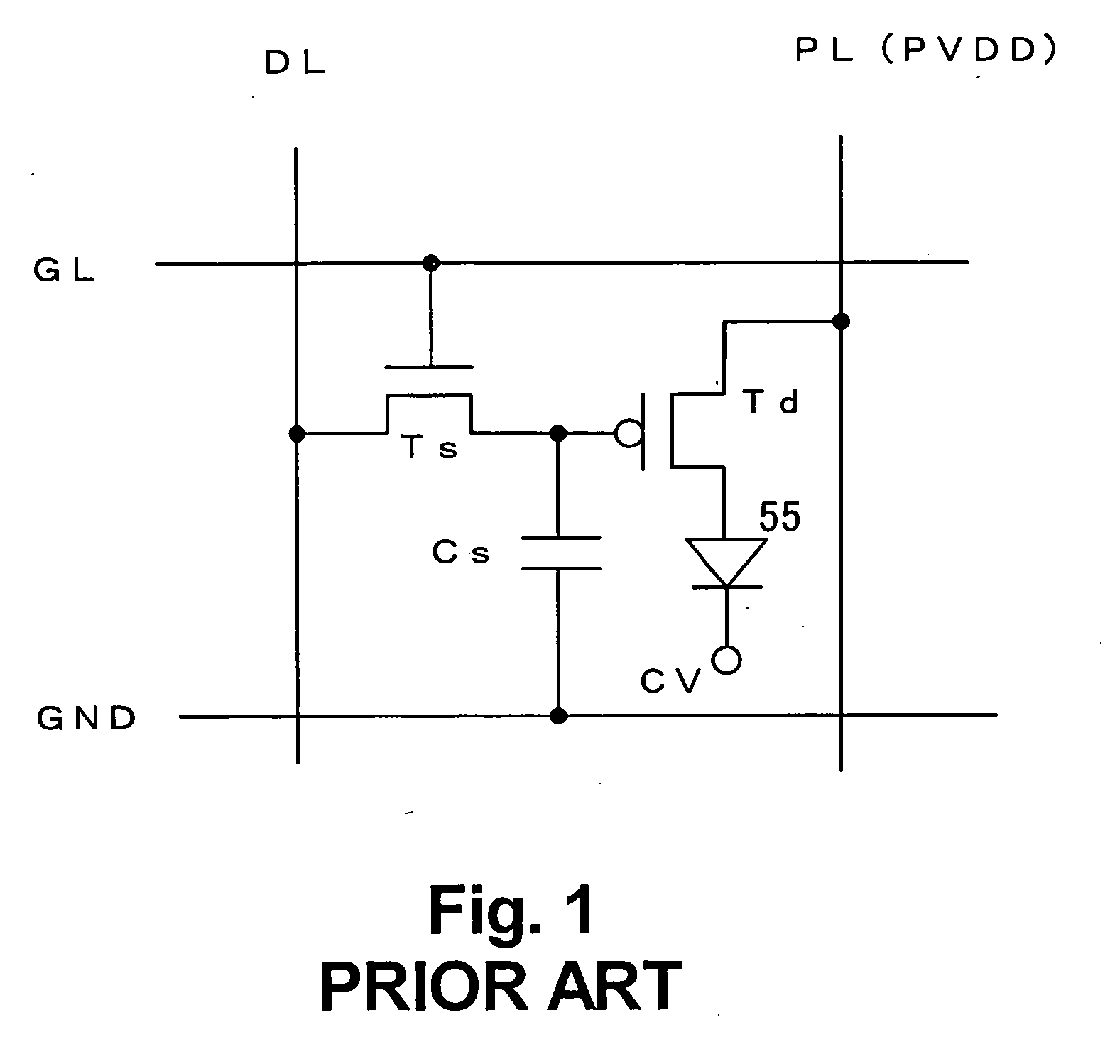
[0054] Each pixel is approximately provided at a region defined by these lines and comprises, as circuit structures, an organic EL element which is an element to be driven, a selection transistor Tr1 which is an n-ch...


PUM


Abstract

In an electroluminescence display device having, on a display panel, a display portion in which pixels are arranged in matrix, an external connection terminal is placed along a lateral side of the display panel and a vertical scan driver circuit is placed on a lateral side of the display panel which opposes the lateral side on which the external connection terminal is placed. Lines for a horizontal scan driver circuit and for the vertical scan driver circuit can be provided only on three sides of the display panel including the side on which the external connection terminal is provided, a side opposing this side, and another side. By not placing the line for the driver circuits on the remaining side, spaces can be secured on this side for a drive current line which supplies power to an electroluminescence element. With this structure, a size of a frame portion can be reduced while securing sufficient width for the drive current common line.

Description

CROSS-REFERENCE TO RELATED APPLICATIONS [0001] The entire disclosures of Japanese Patent Applications Nos. 2005-202992, 2005-202993, and 2005-230129, including their specifications, claims, drawings, and abstracts, are incorporated herein by reference. BACKGROUND OF THE INVENTION [0002] 1. Field of the Invention [0003] The present invention relates to a layout in a display panel in which an electroluminescence element (hereinafter simply referred to as “EL element”) is used as a display element in each of pixels arranged in a matrix. [0004] 2. Description of the Related Art [0005] Display devices which use EL elements, in particular, organic EL elements which are current-driven light emitting elements as a display element in each pixel, are known. Among EL display devices, active matrix display devices in which a transistor (thin film transistor or “TFT”) is provided in each pixel for individually driving, for each pixel, the organic EL element provided in each pixel are now a focus...

Claims


Application Information

Patent Timeline
Patent Type & Authority Applications(United States)
IPC IPC(8): G09G3/36
CPCH01L27/3276H10K59/131H05B33/26H05B33/22
Inventor MATSUMOTO, SHOICHIRO
Owner SANYO ELECTRIC CO LTD
Why Eureka
Try Eureka