Liquid crystal display device and electronic apparatus

a display device and liquid crystal technology, applied in closed circuit television systems, instruments, television systems, etc., can solve the problems of deviation in thickness of retardation or disturbance in alignment of liquid crystal polymers constituting retardation layers, difficulty in obtaining high contrast, and narrow viewing angle at the time of transmissive display. achieve high contrast, wide viewing angle, and high contrast

Inactive Publication Date: 2007-01-18
JAPAN DISPLAY WEST
View PDF6 Cites 32 Cited by
  • Summary
  • Abstract
  • Description
  • Claims
  • Application Information

AI Technical Summary

Benefits of technology

[0009] An advantage of the present invention is to provide a transverse-electric-field mode liquid crystal display device which can provide high-contrast display without being colored at the time of reflective display and can also provide high-contrast display and display with a wide viewing angle at the time of transmissive display.
[0010] According to an aspect of the invention, there is provided a liquid crystal display device comprising a first substrate and a second substrate opposed to each other with a liquid crystal layer therebetween, in which a first electrode and a second electrode are provided on a side of the first substrate opposed to the liquid crystal layer, the liquid crystal layer is driven by means of an electric field generated between the first electrode and the second electrode, and a reflective display area for reflective display and a transmissive display area for transmissive display are formed in a sub pixel area, wherein the thickness of the liquid crystal layer in the reflective display area is greater than the thickness of the liquid crystal layer in the transmissive display area, and wherein a retardation layer is selectively formed in an area corresponding to at least the reflective display area on a side of the second substrate opposed to the liquid crystal layer.
[0011] According to this configuration, incident light from the second substrate can be converted into wide-band circular polarized light by the use of the liquid crystal layer and the retardation layer formed on the side of the second substrate opposed to the liquid crystal layer. Accordingly, it is possible to provide reflective black display with small color, thereby embodying reflective display with high contrast.
[0012] Since the retardation layer is selectively formed in the area on the second substrate opposed to the liquid crystal layer and corresponding to the reflective display area, the same optical design as the transmissive mode is possible in the transmissive display, and it is possible to embody transmissive display with high contrast and a wide viewing angle.
[0013] The area of the second substrate opposed to the liquid crystal layer and corresponding to the reflective display area indicates an area of the second substrate opposed to the liquid crystal layer, where the area two-dimensionally overlaps with the reflective display area as seen two-dimensionally.
[0014] Since the thickness of the liquid crystal layer in the reflective display area is smaller than the thickness of the liquid crystal layer in the transmissive display area, it is possible to make electro-optical characteristics constant in the transmissive display and the reflective display.

Problems solved by technology

However, in the methods described in the above-mentioned known documents, since the reflective black display is colored due to a wavelength dispersion characteristic of a liquid crystal material and a material of the inner retardation layer, it is difficult to obtain high contrast.
In the reference documents of M. O. Choi et al., Y. H. Jeong et al., and Gak Seok Lee et al., since the inner retardation layer is also formed in the transmissive display area, a retardation film is required for the outer surface of the substrate in optical design, thereby causing a problem that a viewing angle at the time of transmissive display is narrowed.
In addition, since the unevenness on the color material layer resulting from the adjustment of chromaticity is made flat by the planarization layer and then the retardation layer is formed thereon, it is difficult to cause deviation in thickness of the retardation or disturbance in alignment of the liquid-crystal polymers constituting the retardation layer.

Method used


Image

  • Liquid crystal display device and electronic apparatus
  • Liquid crystal display device and electronic apparatus
  • Liquid crystal display device and electronic apparatus

Examples


first embodiment

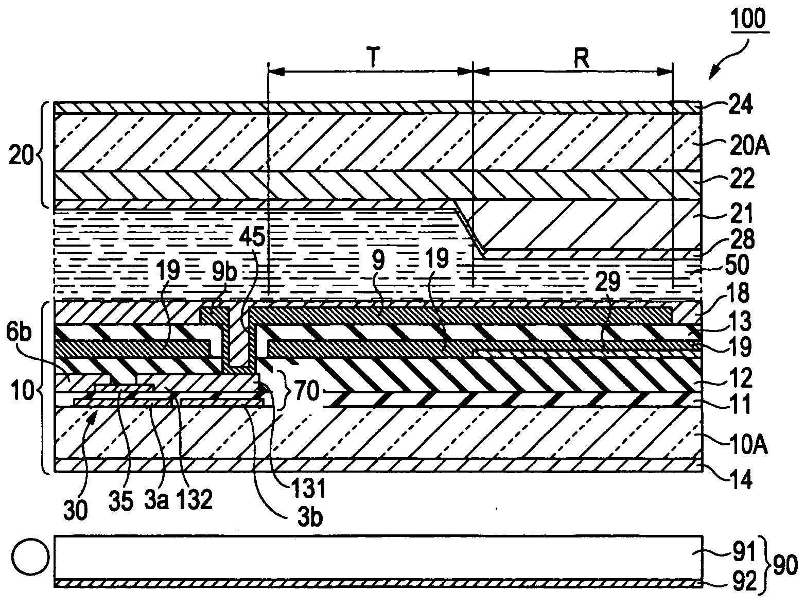
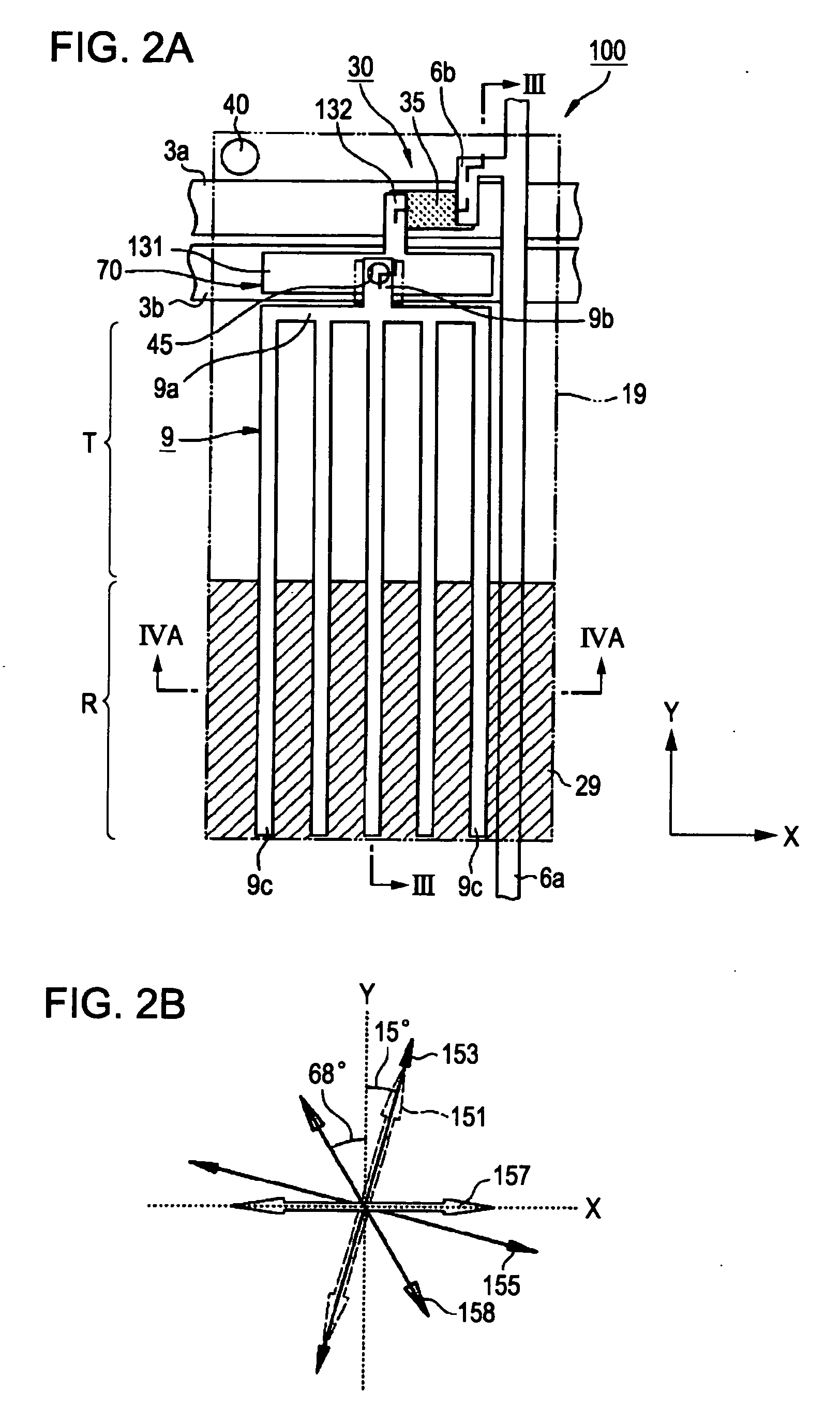
[0039] Hereinafter, a liquid crystal display device according to a first embodiment of the present invention will be described with reference to the drawings. The liquid crystal display device according to the first embodiment employs a fringe field switching (FFS) mode among transverse electric field modes which display an image by applying an electric field (transverse electric field) to liquid crystal molecules in a in-plane direction of a substrate to control alignment of the liquid crystal molecules.

[0040] The liquid crystal display device according to the first embodiment a color liquid crystal display device having a color filter on the substrate, in which three sub pixels emitting colored light components of red (R), green (G), and blue (B) form a pixel. Accordingly, a display area serving as a unit constituting display is referred to as a “sub pixel area” and a display area including a set of sub pixels (R, G, and B) is referred to as a “pixel area.”

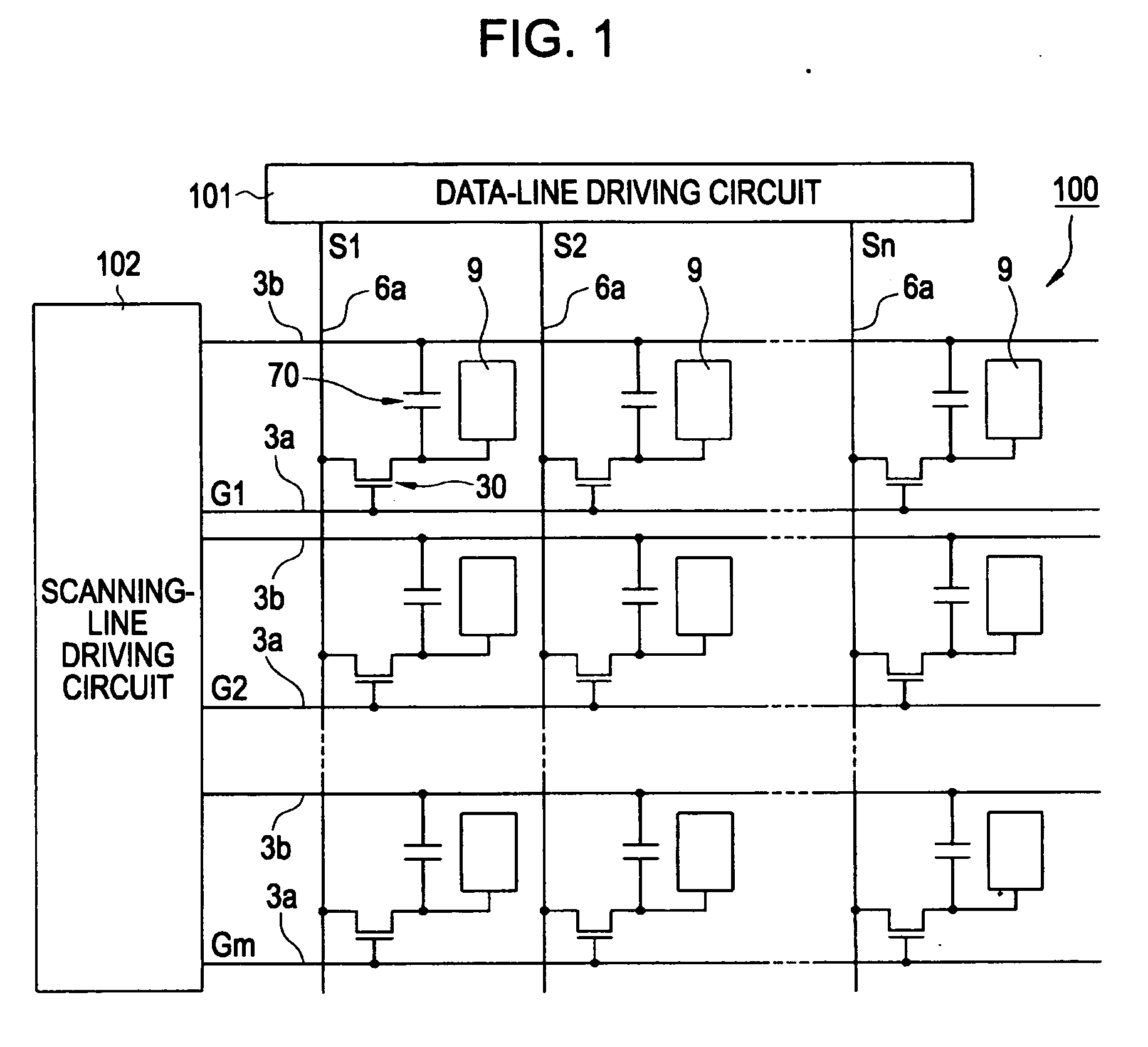
[0041]FIG. 1 is a circu...

second embodiment

[0075] Next, a second embodiment of the invention will be described with reference to the drawings. FIG. 5A is a plan view illustrating a sub pixel area of a liquid crystal display device 200 and FIG. 5B is a diagram illustrating arrangement of optical axes in FIG. 5A. FIG. 6 is a partially sectional view taken along Line D-D′ of FIG. 5A.

[0076] The liquid crystal display device 200 according to the second embodiment has a basic structure substantially similar to that of the liquid crystal display device 100 according to the first embodiment, but is different from the liquid crystal display device 100 in that the pixel electrode 9 and the common electrode 19 are both formed in a pectinated shape as seen two-dimensionally, and band-shaped electrodes (branched electrodes) constituting the pectinated portions and extending in a rod shape are formed in the same layer. In addition, in FIGS. 5, 6, and 7, the same reference numerals denote the same elements as the liquid crystal display de...

third embodiment

[0104] Next, a third embodiment of the invention will be described with reference to FIG. 8. A liquid crystal display device 300 according to the third embodiment has the same basic structure as the liquid crystal display device according to the first embodiment, but is different from the liquid crystal display device according to the first embodiment, in that a resin layer 23 and a retardation layer 21 are stacked in an area on the color filter 22 corresponding to the reflective display area R. Accordingly, the two-dimensional structure of a sub pixel area and the arrangement of optical axes are completely equal to those of the first embodiment and thus description thereof is omitted. In FIG. 8, the same elements as the liquid crystal display device 100 shown in FIGS. 1 to 4 are denoted by the same reference numerals and detailed description thereof is omitted.

[0105]FIG. 8 is a partially sectional view illustrating the liquid crystal display device according to the third embodimen...


PUM

PropertyMeasurementUnit
thickness d1aaaaaaaaaa

Abstract

A liquid crystal display device includes a first substrate and a second substrate opposed to each other with a liquid crystal layer therebetween, in which a first electrode and a second electrode are provided on a side of the first substrate opposed to the liquid crystal layer and the liquid crystal layer is driven by means of an electric field generated between the first electrode and the second electrode. A reflective display area for reflective display and a transmissive display area for transmissive display are formed in a sub pixel area. The thickness of the liquid crystal layer in the reflective display area is greater than the thickness of the liquid crystal layer in the transmissive display area. A retardation layer is selectively formed in an area corresponding to at least the reflective display area on a side of the second substrate opposed to the liquid crystal layer.

Description

[0001] This application claims the benefit of Japanese Patent Application No. 2005-207015 filed Jul. 15, 2005 and Japanese Patent Application No. 2006-16017 filed Jan. 25, 2006. The entire disclosure of the prior applications is hereby incorporated by reference herein their entirety. BACKGROUND [0002] 1. Technical Field [0003] The present invention relates to a liquid crystal display device and an electronic apparatus. [0004] 2. Related Art [0005] A mode (hereinafter, referred to as a “transverse electric field mode”) of controlling alignment of liquid crystal molecules by applying a substrate-in-plane electric field to a liquid crystal layer has been known as a mode of a liquid crystal display device. There have been also known an in-plane switching (IPS) mode and a fringe-field switching (FFS) mode depending upon the shapes of the electrodes for applying an electric field to the liquid crystal layer. Transflective liquid crystal display devices employing the transverse electric fi...

Claims


Application Information

Patent Timeline
Patent Type & Authority Applications(United States)
IPC IPC(8): H04N7/18G02F1/1335H04N9/47
CPCG02F1/133371G02F1/133555G02F2413/09G02F2001/133638G02F1/134363G02F1/133631G02F1/133638G02F1/1335
Inventor TSUCHIYA, HITOSHIMATSUSHIMA, TOSHIHARU
Owner JAPAN DISPLAY WEST
Why Eureka
Try Eureka