High performance mosfet comprising stressed phase change material and method of fabricating the same

a phase change material and high-performance technology, applied in the field of high-performance metaloxidesemiconductor field effect transistors containing stressed phase change materials, can solve the problems of pcm intrinsic stresses (either compressive or tensile stresses)

Inactive Publication Date: 2007-01-25
IBM CORP
View PDF6 Cites 45 Cited by
  • Summary
  • Abstract
  • Description
  • Claims
  • Application Information

AI Technical Summary

Problems solved by technology

The phase change typically leads to volumetric expansion or contraction of the PCM(s), which can, in turn, results in intrinsic stresses (either compressive or tensile stresses) in the PCM(s) if the surrounding environment limits the expansion or contraction.

Method used


Image

  • High performance mosfet comprising stressed phase change material and method of fabricating the same
  • High performance mosfet comprising stressed phase change material and method of fabricating the same
  • High performance mosfet comprising stressed phase change material and method of fabricating the same

Examples


Embodiment Construction

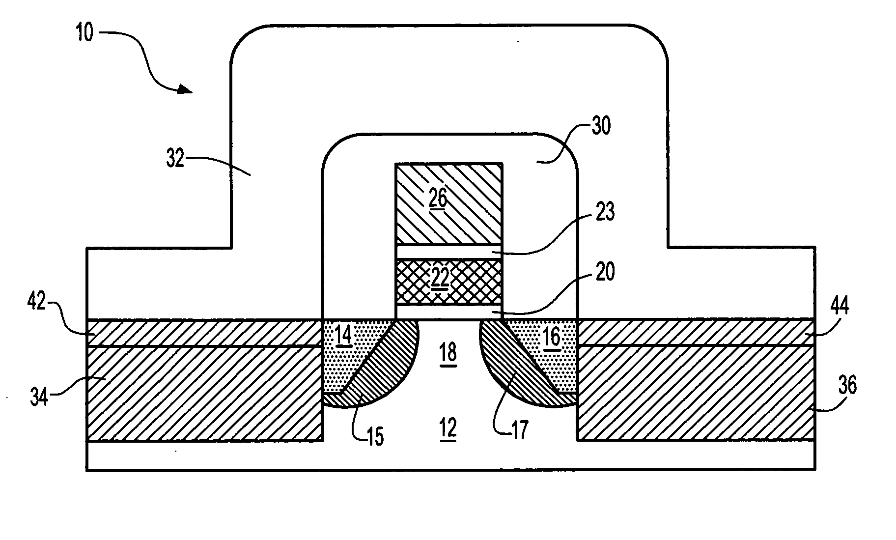
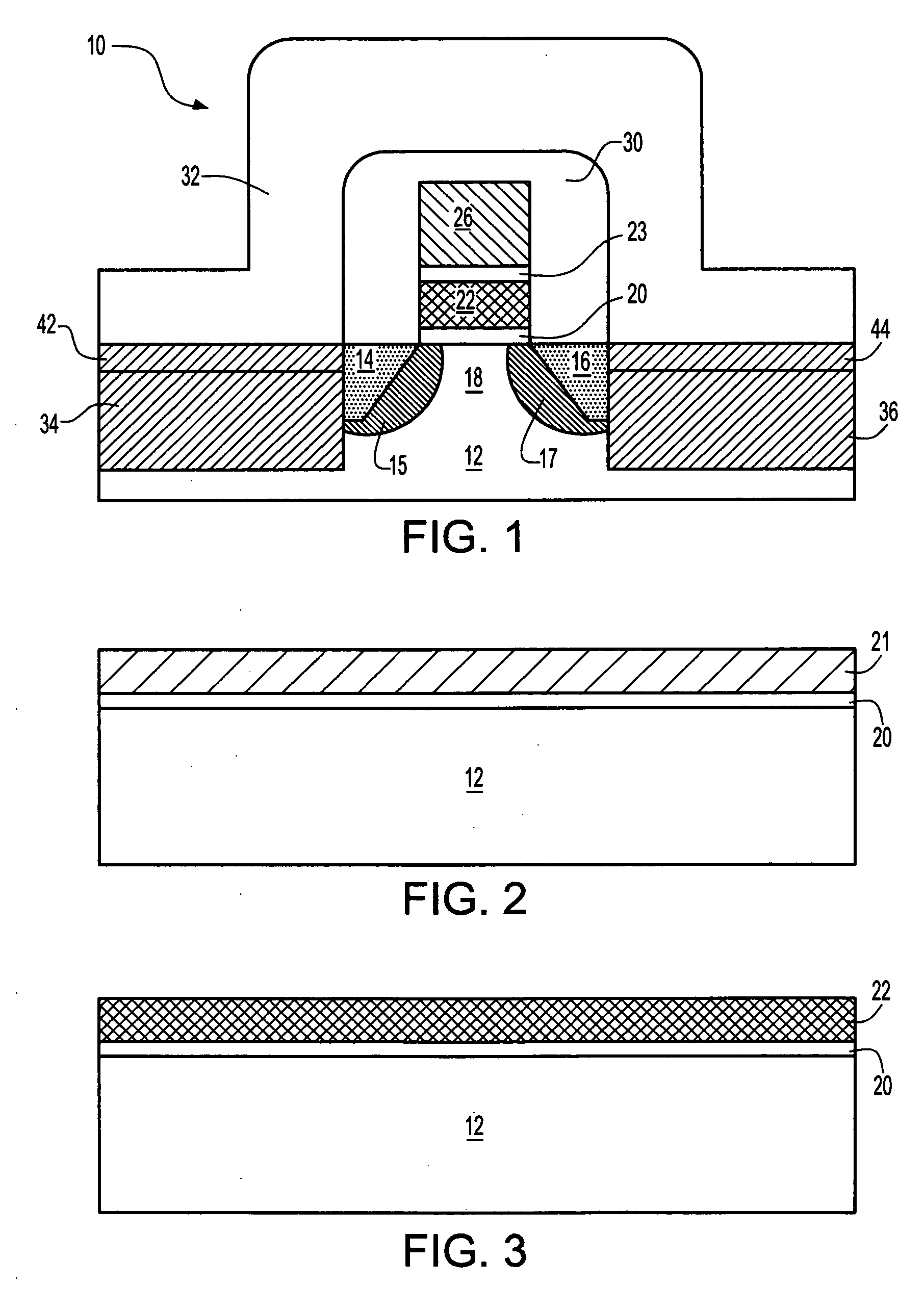
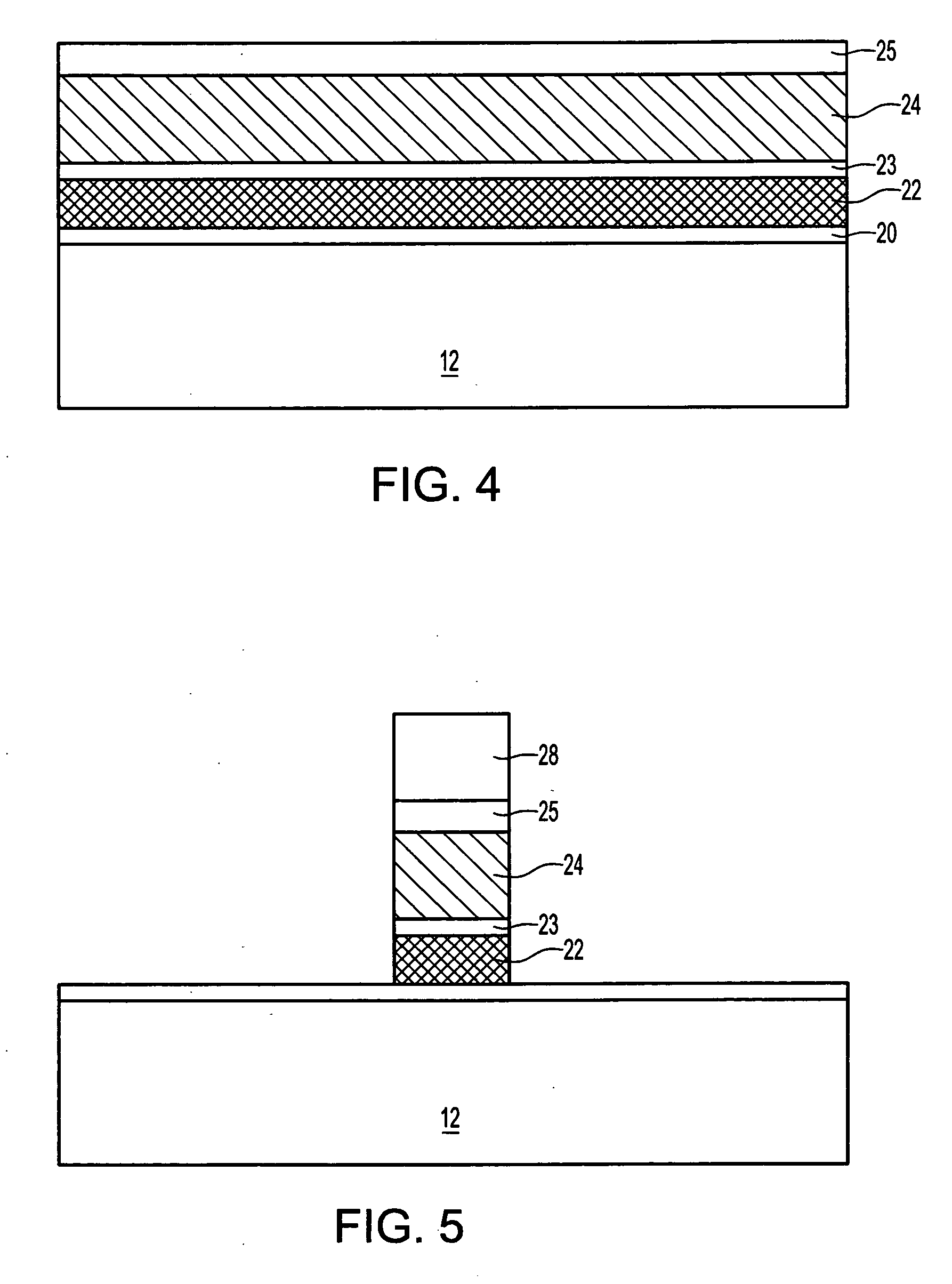
[0024] As mentioned hereinabove, the present invention uses an intrinsically stressed phase change material layer to create desired stress in the channel region of an FET (i.e., tensile stress in an n-channel and compressive stress in a p-channel). The intrinsically stressed phase change material layer is preferably formed from an unstressed phase change material layer via phase change treatment, which results in volumetric expansion or contraction that, in turn, leads to intrinsic compressive or tensile stress in the phase change material layer.

[0025] Phase change materials are well known in the art. For example, chalcogenide materials, such as Ge2Sb2Te5 (GST), In2Se3 (IS), Sb2Te (ST), etc., and other phase change materials comprising groups IV to VI elements have been found reversibly switchable between an amorphous phase and a crystalline phase when heated to different temperatures or when different electrical pulses are applied. Specifically, when heated by an applied electrica...


PUM


Abstract

The present invention relates to semiconductor devices that each comprises at least one field effect transistor (FET) containing an intrinsically stressed phase change material layer. The intrinsically stressed phase change material layer is arranged and constructed for creating stress in the channel region of the FET. Preferably, the intrinsically stressed phase change material layer is deposited over the channel region of the FET. For an n-channel FET, the intrinsically stressed phase change material layer preferably contains intrinsic compressive stress that is created by phase change, for example, from a polycrystalline phase to an amorphous phase. Alternatively, for a p-channel FET, the intrinsically stressed phase change material layer preferably contains intrinsic tensile stress that is created by phase change, for example, from an amorphous phase to a polycrystalline phase.

Description

FIELD OF THE INVENTION [0001] This invention relates to a semiconductor device containing at least one high performance field effect transistor (FET), and more specifically to a high performance metal-oxide-semiconductor field effect transistor (MOSFET) containing a stressed phase change material. The present invention also relates to methods for fabricating such a semiconductor device. BACKGROUND OF THE INVENTION [0002] Mechanical stresses within a semiconductor device substrate can be used to modulate device performance. For example, in silicon, hole mobility is enhanced when the silicon film is under compressive stress, while the electron mobility is enhanced when the silicon film is under tensile stress. Therefore, compressive and / or tensile stresses can be advantageously created in the channel regions of p-channel MOSFETs and / or n-channel MOSFETs, in order to enhance the performance of such p-channel and / or n-channel MOSFETs. [0003] One conventional approach for creating a stre...

Claims


Application Information

Patent Timeline
Patent Type & Authority Applications(United States)
IPC IPC(8): H01L29/76
CPCH01L21/26586H01L27/101H01L29/7843H01L29/665H01L29/6659H01L29/4966
Inventor ZHU, HUILONG
Owner IBM CORP
Why Eureka
Try Eureka