Wafer level package and its manufacturing method

a technology of wafer level and packaging, applied in the direction of electrical equipment, semiconductor devices, semiconductor/solid-state device details, etc., can solve the problems of increased package cost, high package cost, and easy separation of solder balls from wafer level packages, so as to reduce the external stress, absorb external stress, and improve the joint force of solder balls

Inactive Publication Date: 2007-01-25
AMKOR TECH INC DW US
View PDF7 Cites 20 Cited by
  • Summary
  • Abstract
  • Description
  • Claims
  • Application Information

AI Technical Summary

Benefits of technology

[0010] In accordance with one embodiment of the present invention, a semiconductor package includes a semiconductor die having a plurality of bond pads, a first protective layer formed at the periphery of the bond pads of the semiconductor die, Under Bump Metals (UBM) formed at the bond pads of the semiconductor die, a plurality of solder balls wetted to the UBM, and a second protective layer formed at the periphery of the solder balls. The second protective layer includes a thick collar, which is formed from the surface of the solder ball toward its periphery, so that the joint force of the solder ball can be more improved. Further, the second protective layer protects the surface of the wafer from the external environment, and absorbs and alleviates the external stress.

Problems solved by technology

However, in the conventional wafer level package and its manufacturing method, since the protective layer such as the expensive BCB must be separately formed, the cost of the package becomes high as well as the complicated process, such as a coating process, an align process, an exposure process and a develop process and so on is indispensably required due to the photo etching process.
Also, in the conventional wafer level package and its manufacturing method, because the solder balls are simply wetted to the UBM, where the solder balls are mounted on an external device, there is a problem in that the solder balls can be easily separated from the wafer level package on account of the difference of the CTE (Coefficients of Thermal Expansion) by means of the thermal cycling.
However, in this case, since the collar or ring forming process is separately added, the cost of the package is more increased and the manufacturing process of the package is more complicated.

Method used


Image

  • Wafer level package and its manufacturing method
  • Wafer level package and its manufacturing method
  • Wafer level package and its manufacturing method

Examples


Embodiment Construction

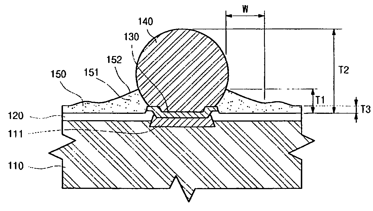
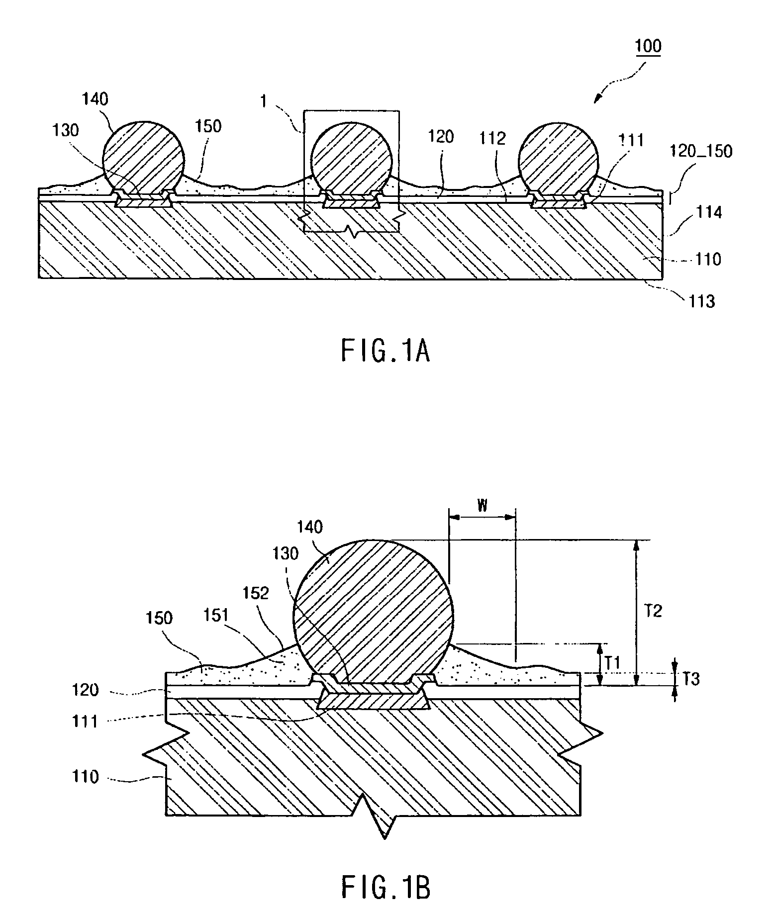
[0016] Referring to FIG. 1A, a sectional view of a wafer level package 100 according to one embodiment of the present invention is illustrated. Referring to FIG. 1B, a sectional view of a part 1 of FIG. 1A is illustrated.

[0017] As shown, the wafer level package 100 according to an embodiment of the present invention includes a semiconductor die 110 having a plurality of bond pads 111, a first protective layer 120 formed at the periphery of the bond pads 111 of the semiconductor die 110, Under Bump Metallurgy, sometimes called Under Bump Metals, (UBM) 130 formed on the bond pads 111 of the semiconductor die 110, a plurality of solder balls 140 wetted to the UBM 130, and a second protective layer 150 formed at the periphery of the solder balls 140, so as to strengthen the joint force of the solder ball 140, protect the surface of the semiconductor die 110 and buffer the stress.

[0018] The semiconductor die 110 includes an approximately planar first surface 112 having the plurality of...


PUM


Abstract

A semiconductor package includes a semiconductor die having a plurality of bond pads, a first protective layer formed at the periphery of the bond pads of the semiconductor die, UBM (Under Bump Metals) formed at the bond pads of the semiconductor die, a plurality of solder balls wetted to the UBM, and a second protective layer formed at the periphery of the solder balls. The second protective layer includes a thick collar, which is formed from the surface of the solder ball toward its periphery, so that the joint force of the solder ball can be more improved. Further, the second protective layer protects the surface of the wafer from the external environment, and absorbs and alleviates the external stress.

Description

BACKGROUND OF THE INVENTION [0001] 1. Field of the Invention [0002] The field of the present invention is related to a wafer level package and its manufacturing method. [0003] 2. Description of Related Art [0004] Generally, a wafer level package is completely packaged in a wafer condition, so that it can reduce the size of the package as the real die size and maximize the productivity thereof. [0005] The wafer level package includes a semiconductor die having a plurality of bond pads, an UBM (Under Bump Metallurgy) formed on the bond pads of the semiconductor die, a plurality of solder balls wetted to the UBM, and a protective layer having a uniform thickness such as BCB (Benzo Cyclo Butene) at the periphery of the solder balls. [0006] Also, in the method for manufacturing the wafer level package, the UBM is formed at the semiconductor die of the wafer and then, the protective layer such as the BCB of a predetermined thickness is formed at the periphery thereof by a photo etching pr...

Claims


Application Information

Patent Timeline
Patent Type & Authority Applications(United States)
IPC IPC(8): H01L23/48
CPCH01L23/3192H01L2224/11334H01L24/11H01L24/12H01L24/94H01L2224/0401H01L2224/13022H01L2224/13099H01L2224/16H01L2224/274H01L2924/01013H01L2924/01014H01L2924/01022H01L2924/01028H01L2924/01029H01L2924/01074H01L2924/01078H01L2924/014H01L2924/05042H01L2924/19041H01L2924/19043H01L2924/01024H01L2924/01033H01L24/02H01L2224/10126H01L24/05H01L24/13
Inventor PARK, IN BAEDO, WON CHULSEO, SEONG MIN
Owner AMKOR TECH INC DW US
Why Eureka
Try Eureka