Apparatus for testing semiconductor circuits
- Summary
- Abstract
- Description
- Claims
- Application Information
AI Technical Summary
Benefits of technology
Problems solved by technology
Method used
Image

Examples
Embodiment Construction
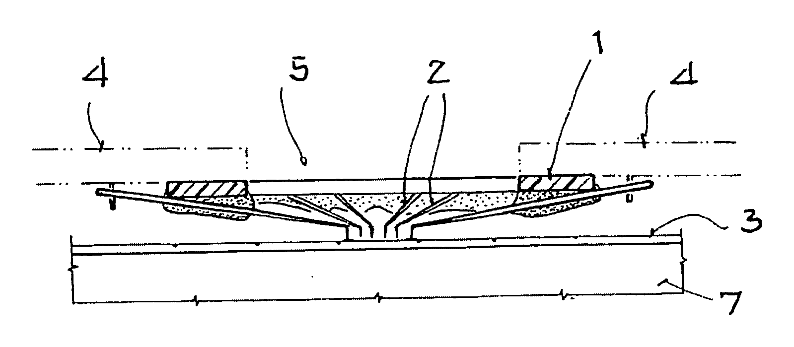
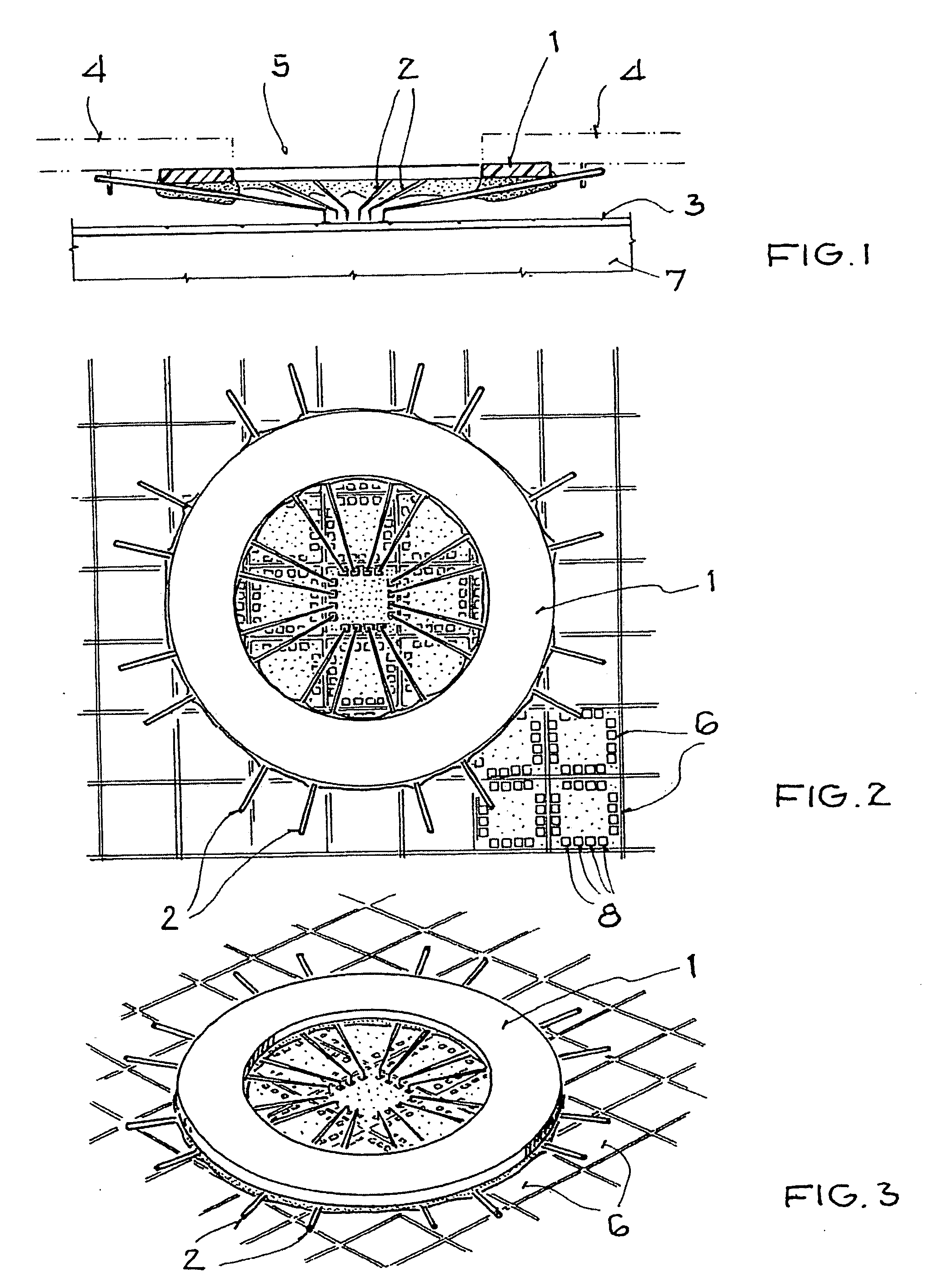
[0031]FIG. 1 shows a section through test head 1 with contact needles 2 during probing of a wafer 3, which is supported on a support device 7. The test head 1 is affixed to the underside of a measurement card 4, which is only shown schematically, and is connected thereto in an electrically conductive manner. The measurement card normally has a circular aperture 5, which affords a view from above of the region of the contact needles 2.
[0032] The top view of the test head 1 in FIG. 2 and its perspective view in FIG. 3 schematically show several components of integrated semiconductor circuits 6 on the wafer 3 and the arrangement of contact areas 8, which are probed by the contact needles 2. The arrangement and number of contact needles 2, as well as the associated circuit arrangement on the measurement card and the shape of the measurement card 4 itself, depend on the electronic components to be tested in each case.
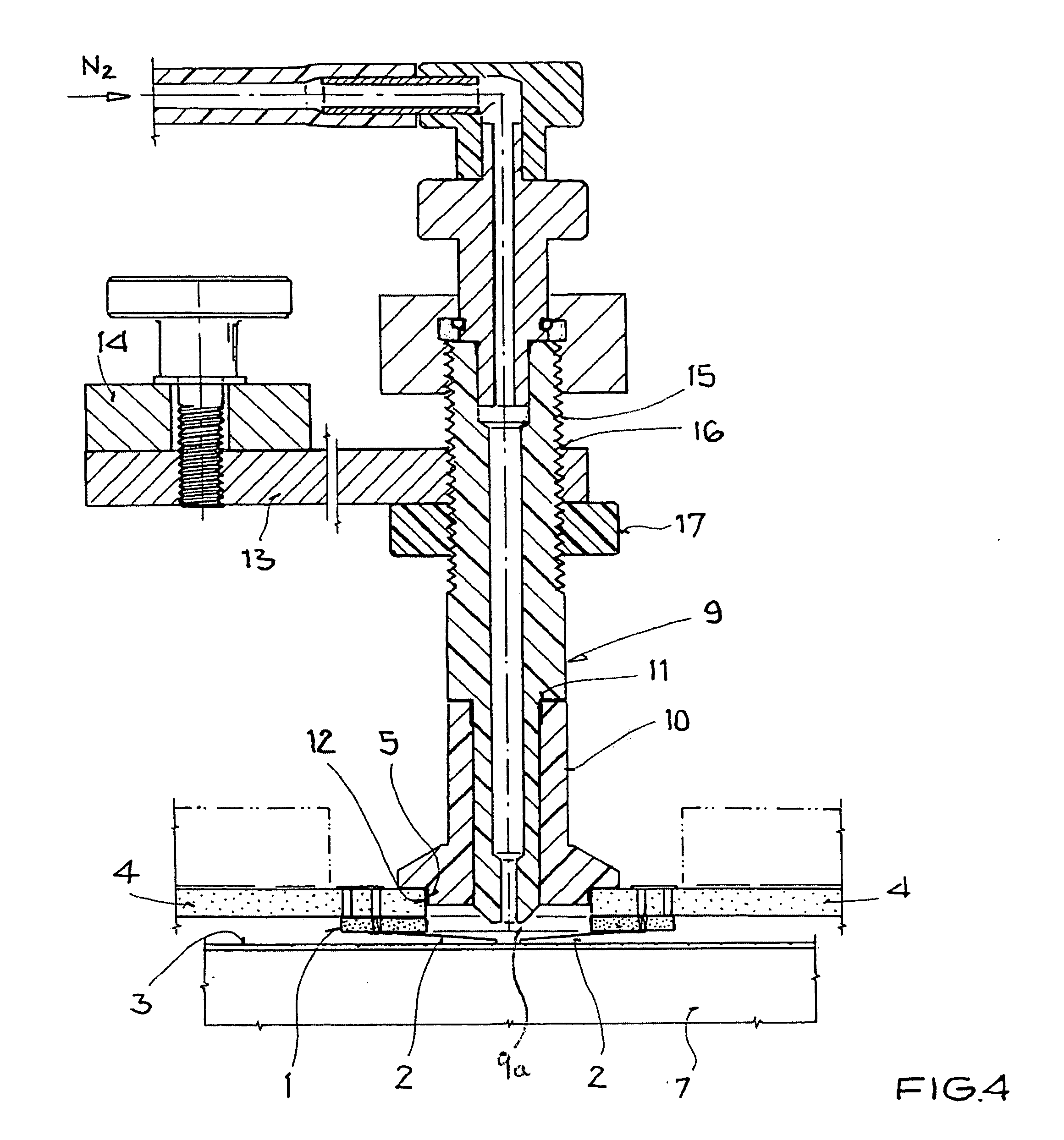
[0033]FIG. 4 shows a section through a nozzle assembly 9 and its atta...
PUM
 Abstract
Description
Claims
Application Information