Read-out circuit in semiconductor memory device

a semiconductor memory and read-out circuit technology, applied in the direction of static storage, digital storage, instruments, etc., can solve the problems of inability to permit a significant freedom of action in the read-out circuit, disadvantageous increase in production cost, and physical sparing of a generous margin of difference between cell current and the current of the cell, so as to reduce the overall length of time required

Inactive Publication Date: 2007-01-25
SHARP KK
View PDF5 Cites 18 Cited by
  • Summary
  • Abstract
  • Description
  • Claims
  • Application Information

AI Technical Summary

Benefits of technology

[0015] The present invention has been developed in view of the foregoing aspects and its object is to provide a read-out circuit in a semiconductor memory device of a time-division sense method which ensures a large margin of the read-out action in a multilevel data storable semiconductor memory device while speeding up the read-out action.

Problems solved by technology

There will hence be difficult for physically sparing a generous margin of difference between the cell current and the reference current.
If the difference between the cell current and the reference current is too small, it may fail to permit a significant freedom of action in the read-out circuit.
Accordingly, the read-out circuit will be enlarged in the installation area and disadvantageously increased in the production cost.
It will hence be difficult to optimize the margin of action during the comparison between the reference voltage and the read-out voltage at each reference current.
On the other hand, the parallel sense method which is disadvantageous in the installation of area includes the sense amplifier for each reference current and can thus optimize the action point of the sense amplifier separately.

Method used


Image

  • Read-out circuit in semiconductor memory device
  • Read-out circuit in semiconductor memory device
  • Read-out circuit in semiconductor memory device

Examples


first embodiment

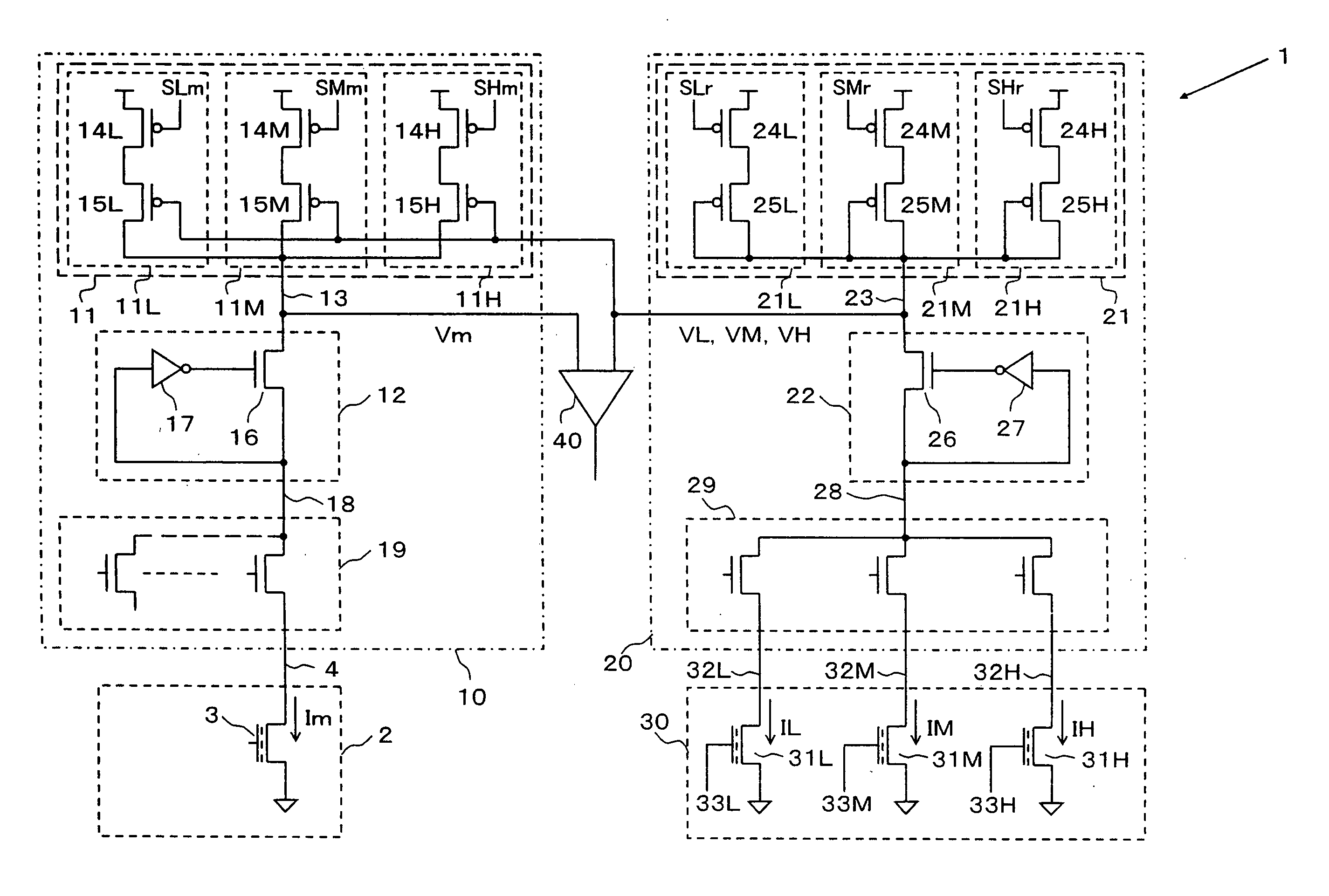
[0044]FIG. 1 is a circuitry diagram of the inventive circuit 1. As shown in FIG. 1, the inventive circuit 1 is a read-out circuit for reading a multilevel data from a selected memory cell 3 in a memory cell array 2 which has multilevel, three or more levels, data storable memory cells arranged in an array, which comprises a read-out voltage generator circuit 10, a reference voltage generator circuit 20, a reference memory cell array 30, and a sense circuit 40. It should be noted that the multilevel data storable memory cells in this embodiment is of a four-level data storable type for ease of the description.

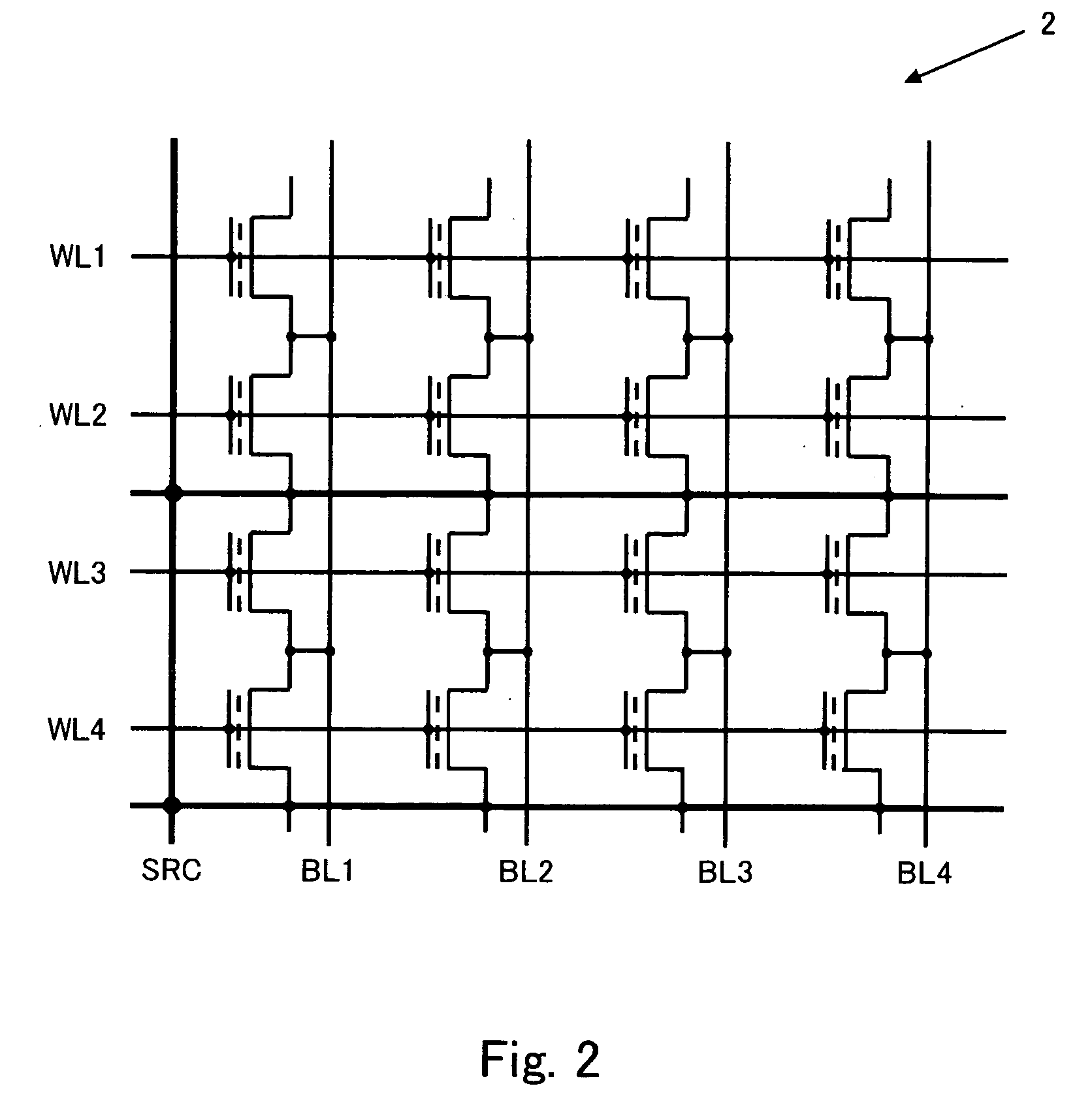
[0045] The memory cell array 2 has memory cells arranged in a matrix consisting of rows and columns, as shown in FIG. 2. The drains of the memory cells along each column are connected to common bit lines BL1 to BL4 which extend along the columns while the gates of the memory cells along each row are connected to common word lines WL1 to WL4 which extend along the rows. The sour...

second embodiment

[0075]FIG. 6 is a circuitry diagram showing an inventive circuit 1 of the second embodiment of the present invention. The inventive circuit 1 shown in FIG. 6 includes a read-out voltage generator circuit 10, a reference voltage generator circuit 20, a reference memory cell array 30, and a sense circuit 40 which are assembled as a read-out circuit for reading a multilevel data from a selected memory cell 3 to be accessed in a memory cell array 2 where a number of multilevel data, three or more levels, storable memory cells are arranged in an array.

[0076] This embodiment is differentiated from the first embodiment by the arrangement of PMOSs 15L, 15M, and 15H in their respective current supply paths 11L, 11M, and 11H of a main loading circuit 11 in the read-out voltage generator circuit 10 and the arrangement of PMOSs 25L, 25M, and 25H in their respective current supply paths 21L, 21M, and 21H of a reference loading circuit 21 in the reference voltage generator circuit 20 which both ...


PUM


Abstract

A read-out circuit comprises a read-out voltage generator circuit converting a memory cell current into a read-out voltage, a reference voltage generator circuit supplying a reference memory cell corresponding to each memory state intermediate between multilevel data with a reference current from a reference loading circuit and converting the reference current flowing through the reference memory cell sequentially selected into a reference voltage. The reference voltage generator circuit modifies the current supply capability of the reference loading circuit corresponding to a change in the selection of the reference memory cell to suppress a change in the reference voltage derived from a change in the reference current and the read-out voltage generator circuit modifies the current supply capability of the main loading circuit corresponding to a change in the selection of the reference memory cell to increase or decrease in proportion to the current supply capability of the reference loading circuit.

Description

CROSS REFERENCE TO RELATED APPLICATION [0001] This Nonprovisional application claims priority under 35 U.S.C. § 119(a) on Patent Application No. 2005-212557 filed in Japan on Jul. 22, 2005, the entire contents of which are hereby incorporated by reference. BACKGROUND OF THE INVENTION [0002] 1. Field of the Invention [0003] The present invention relates to a read-out circuit in a semiconductor memory device for reading a multilevel data of three or more levels from selected memory cells in a memory cell array where a number of multilevel data storable memory cells are arranged in an array. [0004] 2. Description of the Related Art [0005] A typical read-out circuit in a semiconductor memory device is provided for supplying a selected memory cell to be accessed for reading a data with electric current, comparing the (cell) current depending on the data to be read with a reference current to judge whether the cell current is greater or smaller than the reference current, and reading out ...

Claims


Application Information

Patent Timeline
Patent Type & Authority Applications(United States)
IPC IPC(8): G11C16/04G11C11/34G11C16/06
CPCG11C7/062G11C7/067G11C7/1051G11C16/28G11C11/5642G11C2211/5634G11C7/14
Inventor MOTOKI, TOMOHISA
Owner SHARP KK
Why Eureka
Try Eureka