
Method for reducing the trap density in a semiconductor wafer

a technology of trap density and semiconductor wafer, which is applied in the direction of semiconductor/solid-state device manufacturing, basic electric elements, electric devices, etc., can solve the problems of increasing the cost of fga treatment, adding another long treatment at the end of the manufacturing process of the wafer, and not being effective in fga treatment. to achieve the effect of reducing the trap density

Active Publication Date: 2007-01-25
S O I TEC SILICON ON INSULATOR THECHNOLOGIES
View PDF13 Cites 3 Cited by
  • Summary
  • Abstract
  • Description
  • Claims
  • Application Information

AI Technical Summary

Benefits of technology

[0012] This invention provides methods that overcome these problems in the prior art, specifically methods for reducing the trap density at an i...

Problems solved by technology

Therefore, a FGA treatment could be carried out for reducing the DIT at the interface between the active layer and the underlying oxide layer in a SOI-type wafer, but this FGA treatment would not be effective if wafer is covered by a capping oxide layer.
Therefore, FGA treatment does not appear as a solution to reducing DIT at the interface between the active layer and the underlying layer in the presence of a capping layer.
But such treatment would mean adding another lengthy treatment at the end of the manufacturing process of the wafer, which is of course not desired.
Although, this could reduce DIT at the interface between an active layer and an adjacent insulating (e.g. oxide) layer, reductions are not observed in practice.

Method used


Image

  • Method for reducing the trap density in a semiconductor wafer
  • Method for reducing the trap density in a semiconductor wafer

Examples


examples

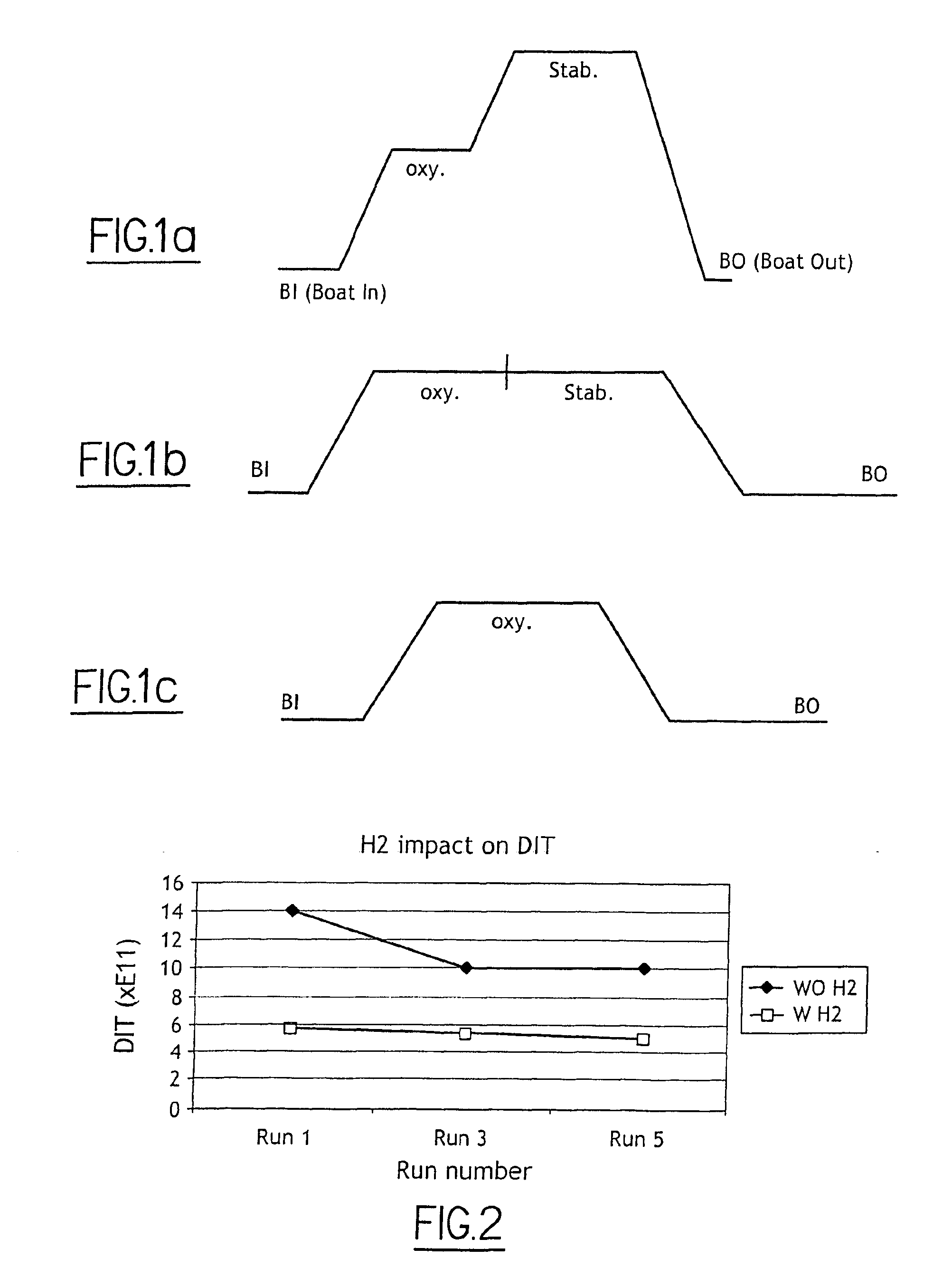
[0051]FIG. 2 illustrates results of experiments conducted by the inventors on SOI wafers fabricated by a method based on the SMART-CUT® technology. This figure shows the value of the DIT measured on groups of otherwise identical wafers, labelled respectively to “run1”, “run2” and “run3”, that have been processed under the same conditions, except for the presence and absence of H2 and except for different boat-out, or final, temperatures:

[0052] run1: with and without H2 at a boat-out temperature of 450° C.,

[0053] run2: with and without H2 at a boat-out temperature of 600° C.,

[0054] run3: with and without H2 at a boat-out temperature of 750° C.

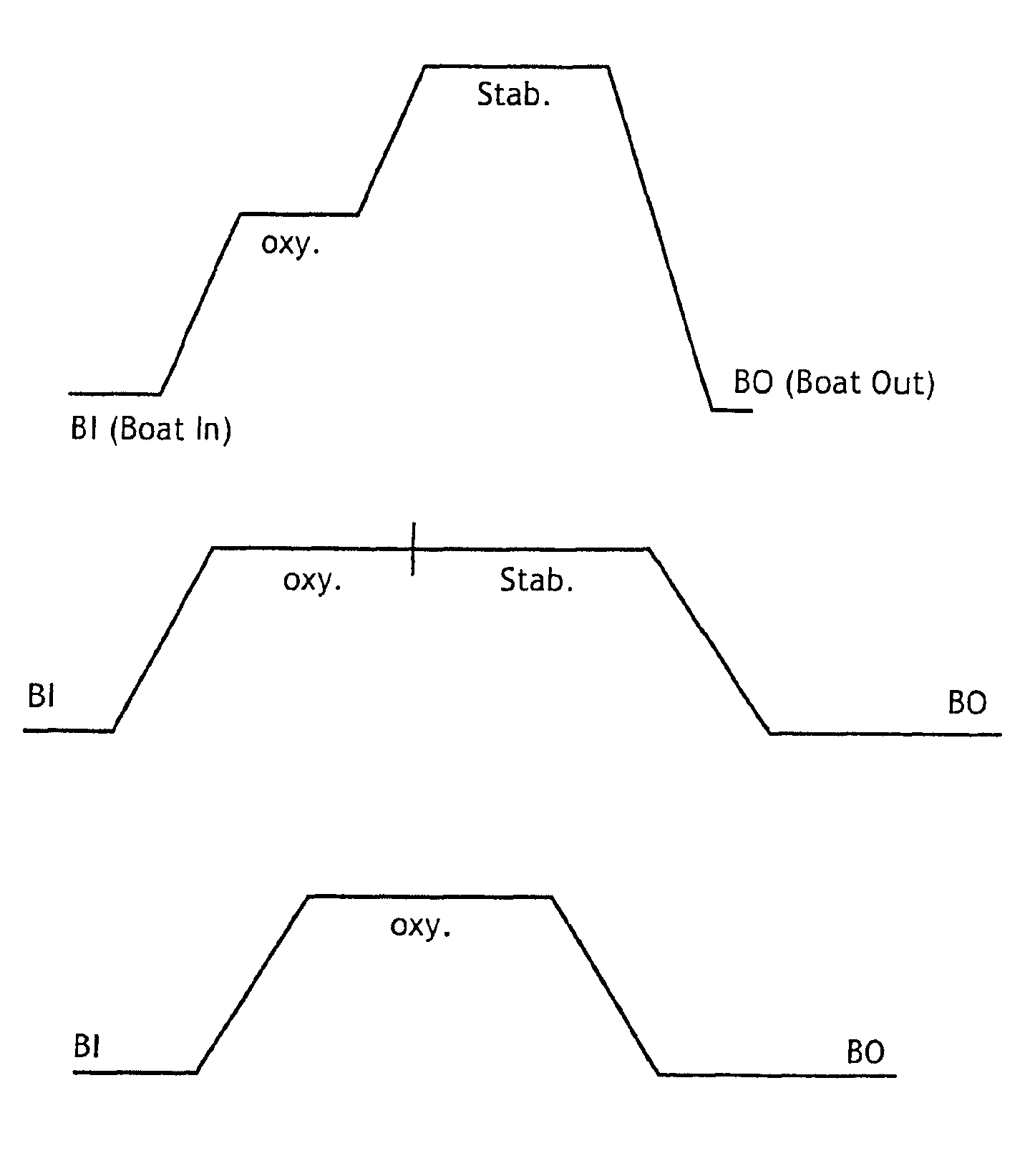
[0055] All runs included a starting phase followed by an oxidation phase at 950° C. and then by a stabilizing phase at a temperature of about 1100° C. The DIT measurements were carried out in the same manner for all runs.

[0056]FIG. 2 illustrates two curves, each curve defined by three points (a point for each group or “run”). The upper curv...


PUM


Abstract

The invention provides methods for reducing trap densities at interfaces in a multilayer semiconductor wafer, specifically trap densities between an active layer and an insulating layer under the active layer. The methods comprise exposing wafers to high temperatures in a generally neutral atmosphere that also comprises one or more species that can, or whose ions can, migrate into the wafer down to the interface where reduction of the trap density is desired.

Description

CROSS-REFERENCE TO RELATED APPLICATIONS [0001] This application is a continuation of International application PCT / IB2005 / 000434 filed Feb. 3, 2005, the entire content of which is expressly incorporated herein by reference thereto.FIELD OF THE INVENTION [0002] The invention is directed to reducing trap densities at interfaces within a multilayer semiconductor wafer. The applies many types of multilayer wafer made with semiconductor materials (“semiconductor wafers”), and is particularly advantageous for multilayer semiconductor wafers fabricated by a transfer method, and is more particularly advantageous for SOI-type wafers. BACKGROUND OF THE INVENTION [0003] DIT is a parameter that represents the density interface traps that limit the mobility of electrical carriers in the multilayer wafers, and carrier mobility has a key influence on the electrical performance of a multilayer wafer. As an example, traps represented by DIT values at a BOX / active layer interface of a SOI wafer affec...

Claims


Application Information

Patent Timeline
IPC IPC(8): H01L21/30H01L21/46
CPCH01L21/324H01L21/28167
Inventor BRUNIER, FRANCOISRENAULD, VIVIENWAECHTER, JEAN MARC
Owner S O I TEC SILICON ON INSULATOR THECHNOLOGIES
Learn More