Structure and a manufacturing method of a mosfet with an element of iva group ion implantation

a manufacturing method and metal oxide technology, applied in the direction of basic electric elements, electrical equipment, semiconductor devices, etc., can solve the problems of low field-effect mobility and the major drawback of transistors of silicon carbide elements, and achieve the effect of enhancing field-effect mobility and improving the quality of gate oxide layers

Active Publication Date: 2020-01-30
NATIONAL TSING HUA UNIVERSITY
View PDF0 Cites 0 Cited by
  • Summary
  • Abstract
  • Description
  • Claims
  • Application Information

AI Technical Summary

Benefits of technology

[0007]The invention provides a structure and a manufacturing method of a metal-oxide-semiconductor field-effect transistor with an element of IVA group ion implantation to improve the quality of the gate oxide layer and enhance the field-effect mobility.

Problems solved by technology

In the prior art, the too low field-effect mobility (5 to 10 cm2 / V·s) of the silicon carbide metal-oxide-semiconductor field-effect transistor is always the major drawback of the silicon carbide element.

Method used


Image

  • Structure and a manufacturing method of a mosfet with an element of iva group ion implantation
  • Structure and a manufacturing method of a mosfet with an element of iva group ion implantation
  • Structure and a manufacturing method of a mosfet with an element of iva group ion implantation

Examples


Embodiment Construction

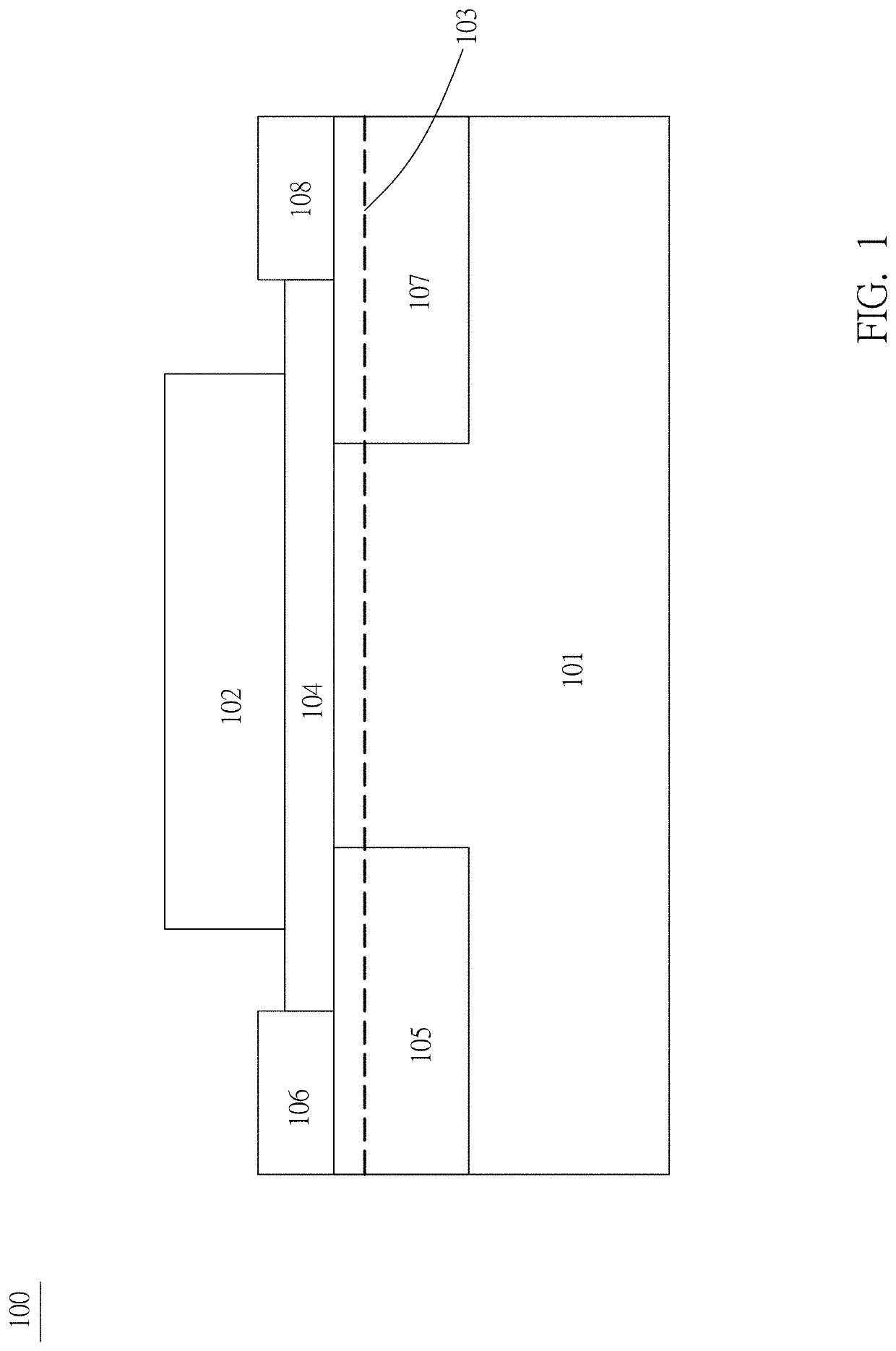
[0022]FIG. 1 is a schematic view showing a structure of a metal-oxide-semiconductor field-effect transistor with an element of IVA group ion implantation according to an embodiment of the invention. Referring to FIG. 1, the structure 100 includes a body 101, a gate electrode 102, an element of IVA group ion implantation layer 103, a gate oxide layer 104, a source layer 105, a source electrode 106, a drain layer 107 and a drain electrode 108.

[0023]The gate oxide layer 104 is disposed between the gate electrode 102 and the body 101. The element of IVA group ion implantation layer 103 is disposed in the body 101, and is close to the interface between the gate oxide layer 104 and the body 101, as represented by the dashed line. The element of IVA group ion implantation layer 103 is utilized to change a property of a channel. In one embodiment, the element of IVA group ion implantation layer 103 is utilized to increase the electron mobility of the channel of the structure 100, and is not...


PUM

PropertyMeasurementUnit
depthaaaaaaaaaa
electron mobilityaaaaaaaaaa

Abstract

A structure and a manufacturing method of a metal-oxide-semiconductor field-effect transistor with an element of IVA group ion implantation are disclosed. The element of IVA group ion implantation layer is disposed in a body and close to an interface between a gate oxide layer and the body. The element of IVA group ion implantation layer is utilized to change a property of a channel of the structure.

Description

CROSS-REFERENCE TO RELATED APPLICATIONS[0001]This application claims priority of No. 107125645 filed in Taiwan R.O.C. on Jul. 25, 2018 under 35 USC 119, the entire content of which is hereby incorporated by reference.BACKGROUND OF THE INVENTIONField of the Invention[0002]The invention relates to a structure and a manufacturing method of a metal-oxide-semiconductor field-effect transistor with an element of IVA group ion implantation, and more particularly to a structure and a manufacturing method using an element of IVA group ion implantation to improve oxidation of 4H—SiC before oxidation of a gate oxide layer.Description of the Related Art[0003]In the prior art, the too low field-effect mobility (5 to 10 cm2 / V·s) of the silicon carbide metal-oxide-semiconductor field-effect transistor is always the major drawback of the silicon carbide element. Recently, the use of nitric oxide thermal annealing after oxidation has been developed to effectively increase the electron mobility to ab...

Claims


Application Information

Patent Timeline
Patent Type & Authority Applications(United States)
IPC IPC(8): H01L29/66H01L29/51H01L21/265H01L29/417
CPCH01L29/41766H01L29/66681H01L21/26586H01L29/517H01L29/41783H01L21/26513H01L29/1033H01L29/66477H01L29/78H01L21/049H01L29/1054H01L29/1608H01L29/66068H01L29/7802H01L29/7813H01L21/046H01L21/26506H01L21/425H01L21/8213H01L21/823412H01L29/66537H01L29/7816
Inventor HUANG, CHIH-FANGJIANG, JHENG-YIWANG, SHENG-HONGHUNG, JIA-QING
Owner NATIONAL TSING HUA UNIVERSITY
Why Eureka
Try Eureka