
Trans-organic thin film solar cell modified by polarity buffer layer

A technology of solar cells and organic thin films, applied in circuits, photovoltaic power generation, electrical components, etc., can solve the problems of large series resistance of devices, limiting short-circuit current density, and high carrier trap density, etc., to increase short-circuit current density, The effect of promoting vertical phase separation and reducing trap density

Inactive Publication Date: 2014-07-23
UNIV OF ELECTRONICS SCI & TECH OF CHINA
View PDF2 Cites 0 Cited by
  • Summary
  • Abstract
  • Description
  • Claims
  • Application Information

AI Technical Summary

Problems solved by technology

[0004] However, in the inverted structure solar cell, the main limiting factors of PEDOT:PSS are: 1. The work function mismatch between the anode buffer layer PEDOT:PSS and the metal anode makes it impossible to form an ohmic contact between them, resulting in a large series resistance of the device, and finally The short-circuit current density is limited; 2. The polarity of the solvent of the anode buffer layer and the solvent of the photoactive layer is different, resulting in uneven film formation on the surface of the photoactive layer, which will lead to an excessive density of carrier traps on the surface of the anode buffer layer, thereby increasing The recombination probability of carriers is increased; 3. The hydrophobic and conductive PEDOT groups and the hydrophilic and non-conductive PSS groups cannot effectively conduct vertical phase separation during the film formation process, thus limiting the carrier transport efficiency

Method used


Image

  • Trans-organic thin film solar cell modified by polarity buffer layer
  • Trans-organic thin film solar cell modified by polarity buffer layer
  • Trans-organic thin film solar cell modified by polarity buffer layer

Examples


Embodiment 1

[0020] Embodiment 1 (control group):

[0021] Clean the substrate composed of transparent substrate and transparent conductive cathode ITO with surface roughness less than 1nm, and blow dry with nitrogen after cleaning; spin-coat ZnO (5000rpm, 40s, 15nm) on the surface of transparent conductive cathode ITO to prepare cathode buffer layer, and bake the formed film (200°C, 60min); prepare P3HT:PCBM (1:20, 20mg / ml) photoactive layer (1000rpm, 25s, 220nm) on the cathode buffer layer by spin coating, and bake (140°C, 5min); spin-coat PEDOT:PSS solution on the surface of the photoactive layer to prepare an anode buffer layer (3000rpm, 60s, 30nm); anneal the substrate by heating and annealing on a constant temperature hot table (150°C ,5min); Evaporate metal anode Ag (100nm) on the anode buffer layer. Under standard test conditions: AM1.5, 100mW / cm 2 , the open circuit voltage of the device was measured (V OC )=0.56V, short-circuit current (J SC )=8.2mA / cm 2 , fill factor (FF)=0...

Embodiment 2

[0023] Clean the substrate composed of transparent substrate and transparent conductive cathode ITO with surface roughness less than 1nm, and blow dry with nitrogen after cleaning; spin-coat ZnO (5000rpm, 40s, 15nm) on the surface of transparent conductive cathode ITO to prepare cathode buffer layer, and bake the formed film (200°C, 60min); prepare P3HT:PCBM (1:20, 20mg / ml) photoactive layer (1000rpm, 25s, 220nm) on the cathode buffer layer by spin coating, and bake (140°C, 5min); spin-coat PEDOT:PSS solution on the surface of the photoactive layer to prepare an anode buffer layer (3000rpm, 60s, 30nm); spin-coat a polar buffer layer on the anode buffer layer (N, N-dimethylformamide 93%, PEODT:PSS7%, 5000rpm, 60s, 5nm); the substrate is annealed by heating and annealing on a constant temperature hot stage (150°C, 5min); metal is evaporated on the polar buffer layer Anode Ag (100nm). Under standard test conditions: AM1.5, 100mW / cm 2 , the open circuit voltage of the device was...

Embodiment 3

[0025] Clean the substrate composed of transparent substrate and transparent conductive cathode ITO with surface roughness less than 1nm, and blow dry with nitrogen after cleaning; spin-coat ZnO (5000rpm, 40s, 15nm) on the surface of transparent conductive cathode ITO to prepare cathode buffer layer, and bake the formed film (200°C, 60min); prepare P3HT:PCBM (1:20, 20mg / ml) photoactive layer (1000rpm, 25s, 220nm) on the cathode buffer layer by spin coating, and bake (140°C, 5min); spin-coat PEDOT:PSS solution on the surface of the photoactive layer to prepare an anode buffer layer (3000rpm, 60s, 30nm); spin-coat a polar buffer layer on the anode buffer layer (N, N-dimethylformamide 95%, PEODT:PSS5%, 5000rpm, 60s, 5nm); the substrate is annealed by heating and annealing on a constant temperature hot table (150°C, 5min); metal is evaporated on the polar buffer layer Anode Ag (100nm). Under standard test conditions: AM1.5, 100mW / cm 2 , the open circuit voltage of the device was...


PUM


Abstract

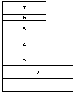
The invention discloses a trans-organic thin film solar cell modified by a polarity buffer layer, and belongs to the field of organic polymer photovoltaic devices or organic semiconductor thin film solar cells. A trans-structure is adopted for the cell, and a substrate, a transparent conductive cathode ITO, a cathode buffer layer, a light active layer, an anode buffer layer, the polarity buffer layer and a metal anode are arranged from bottom to top; the polarity buffer layer comprises, by mass, 93 percent to 97 percent of N, N- dimethyl formamide, three percent to seven persent of poly (3, 4- ethylene thiophene two oxygen radicals)-poly (styrene sulfonic acid), and the thickness of the polarity buffer layer ranges from 1 nm to 10 nm. The polarity buffer layer is added between the anode buffer layer and the metal anode, so that the work function of the anode buffer layer is improved, device series resistance is reduced, the film forming process of the anode buffer layer is optimized, charge carrier composite probability is reduced, the vertical phase separation degree of PEDOT: PSS thin film is promoted, transmission efficiency of the charge carrier is improved, and the photoelectric conversion efficiency of the device is improved.

Description

technical field [0001] The invention belongs to the field of organic polymer photovoltaic devices or organic semiconductor thin-film solar cells, and in particular relates to an organic thin-film solar cell. Background technique [0002] With the explosive growth of the global energy demand, the energy problem has become the primary problem faced by the economic development of all countries. Because solar energy is clean, widely distributed, and inexhaustible, research on photovoltaic power generation to solve energy problems has become the focus and focus of research in the field of renewable energy. Currently, active layer materials can be classified into inorganic semiconductor materials and organic semiconductor materials according to the different properties of materials that make up the photoactive layer of a solar cell. Compared with inorganic semiconductor materials, organic semiconductor materials not only have relatively mild synthesis conditions and device proces...

Claims


Application Information

Patent Timeline
Patent Type & Authority Applications(China)
IPC IPC(8): H01L51/42H01L51/46
CPCH10K30/20H10K30/81Y02E10/549
Inventor 于军胜施薇李曙光王瀚雨
Owner UNIV OF ELECTRONICS SCI & TECH OF CHINA
Learn More