Unlock instant, AI-driven research and patent intelligence for your innovation.

Finfet gate formed of carbon nanotubes

a carbon nanotube and gate technology, applied in the direction of nanotechnology, electrical equipment, semiconductor devices, etc., can solve the problem of difficult to form gate conductor features on finfet structures

Inactive Publication Date: 2007-02-01
IBM CORP
View PDF16 Cites 36 Cited by
  • Summary
  • Abstract
  • Description
  • Claims
  • Application Information

AI Technical Summary

Benefits of technology

[0005] In view of the foregoing, an embodiment of the invention provides a fin field effect transistor (FinFET) gate comprising a semiconductor wafer; a gate dielectric layer over the semiconductor wafer; a conductive material on the gate dielectric layer; an activated carbon nanotube on a surface of the conductive material; and a plated metal layer on the activated carbon nanotube. Preferably, the carbon nanotube is on a sidewall of the conductive material. The conductive material comprises a first metal layer over the gate dielectric

Problems solved by technology

It is often difficult to form gate conductor features on FinFET structures due to the large topography of the fin.

Method used


Image

  • Finfet gate formed of carbon nanotubes
  • Finfet gate formed of carbon nanotubes
  • Finfet gate formed of carbon nanotubes

Examples


Embodiment Construction

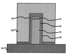
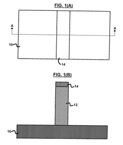
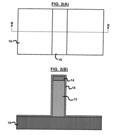
[0060] The embodiments of the invention and the various features and advantageous details thereof are explained more fully with reference to the non-limiting embodiments that are illustrated in the accompanying drawings and detailed in the following description. It should be noted that the features illustrated in the drawings are not necessarily drawn to scale. Descriptions of well-known components and processing techniques are omitted so as to not unnecessarily obscure the embodiments of the invention. The examples used herein are intended merely to facilitate an understanding of ways in which the embodiments of the invention may be practiced and to further enable those of skill in the art to practice the embodiments of the invention. Accordingly, the examples should not be construed as limiting the scope of the embodiments of the invention.

[0061] As mentioned, there remains a need for novel techniques of forming the gate conductor on the FinFETs, which can avoid the requisite lon...


PUM


Abstract

A fin field effect transistor (FinFET) gate comprises a semiconductor wafer; a gate dielectric layer over the semiconductor wafer; a conductive material on the gate dielectric layer; an activated carbon nanotube on a surface of the conductive material; and a plated metal layer on the activated carbon nanotube. Preferably, the carbon nanotube is on a sidewall of the conductive material. The conductive material comprises a first metal layer over the gate dielectric layer, wherein the first metal layer acts as a catalyst for growing the carbon nanotube, wherein the first metal layer is preferably in a range of 1-10 nm in thickness. The semiconductor wafer may comprise a silicon on insulator wafer. The FinFET gate may further comprise a second metal layer disposed between the first metal layer and the gate dielectric layer.

Description

BACKGROUND [0001] 1. Field of the Invention [0002] The embodiments of the invention generally relate to microelectronic logic devices and methods of fabrication and, more particularly, to the design and manufacturing of integrated circuit devices having fin field effect transistor (FinFET) components. [0003] 2. Description of the Related Art [0004] It is often difficult to form gate conductor features on FinFET structures due to the large topography of the fin. If subtractive etch processes are used, very long etch times are typically required, which may introduce variations in the dimensions of the gate conductor itself. Therefore, it is desirable to develop techniques of forming the gate conductor on the FinFETs, which can avoid the requisite long etch times generally found in conventional processes. SUMMARY [0005] In view of the foregoing, an embodiment of the invention provides a fin field effect transistor (FinFET) gate comprising a semiconductor wafer; a gate dielectric layer ...

Claims


Application Information

Patent Timeline
IPC IPC(8): H01L27/12
CPCB82Y10/00H01L29/4908H01L51/0512H01L29/785H01L51/0048H01L29/66795H10K85/221H10K10/462
Inventor FURUKAWA, TOSHIHARUHAKEY, MARK C.HOLMES, STEVEN J.HORAK, DAVID V.KOBURGER, CHARLES W. III
Owner IBM CORP