Data driving circuit and driving method of light emitting display using the same
a driving circuit and data technology, applied in the field of data driving circuits, can solve problems such as the inability to display images of a desired brightness
- Summary
- Abstract
- Description
- Claims
- Application Information
AI Technical Summary
Benefits of technology
Problems solved by technology
Method used
Image
Examples
first embodiment
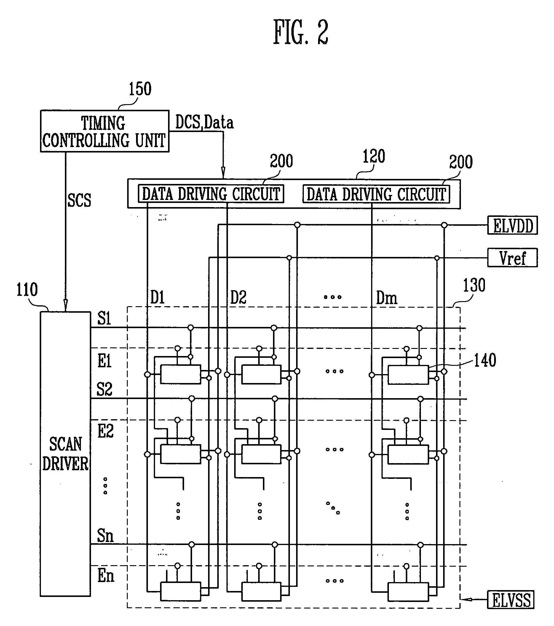
[0074]FIG. 6 is a block diagram showing the data driving circuit 200 shown in FIG. 2. It is assumed that the data driving circuit 200 has an integral j number of channels (wherein j is at least 2) for convenience of the description.
[0075] Referring to FIG. 6, the data driving circuit 200 according to the first embodiment of the present invention includes a shift resistor unit 210, a sampling latch unit 220, a holding latch unit 230, a gamma voltage unit 240, a digital-analog converting unit 250 (hereinafter, referred to as a DAC unit), a first buffer unit 270, a second buffer unit 260, a current supplying unit 280, and a selecting unit 290.
[0076] The shift resistor unit 210 receives the source shift clock (SSC) and source start pulse (SSP) from the timing controlling unit 150. The shift resistor unit 210 receiving the source shift clock (SSC) and the source start pulse (SSP) from the timing controlling unit 150 sequentially generates the j number of the sampling signals by shifting...
third embodiment
[0127]FIG. 12 is a block diagram showing the data driving circuit 200 as shown in FIG. 2. In FIG. 12, elements that have the same reference numerals as in FIG. 6 are configured substantially the same, and therefore their detailed descriptions are omitted.
[0128] Referring to FIG. 12, the data driving circuit 200 according to the third embodiment of the present invention includes the shift resistor unit 210, the sampling latch unit 220, the holding latch unit 230, the DAC unit 250, the first buffer unit 270, the second buffer unit 260, the current supplying unit 280, the selecting unit 290, a gamma voltage unit 400, and a boosting block 410.
[0129] The gamma voltage unit 400 includes j number of voltage generating units 4001 to 400j for generating a predetermined enhancement voltage to correspond to k bits of the data. Each of the voltage generating units 4001 to 400j is composed of a plurality of partial potential resistances (R1 to Rl) to generate the 2k number of enhancement voltag...
fifth embodiment
[0143]FIG. 16 is a block diagram showing the data driving circuit shown in FIG. 2. In FIG. 16, elements that have the same reference numerals as in FIG. 6 are configured substantially the same, and therefore their detailed descriptions are omitted.
[0144] Referring to FIG. 16, the data driving circuit 200 according to the fifth embodiment of the present invention includes the shift resistor unit 210, the sampling latch unit 220, the holding latch unit 230, the gamma voltage unit 240, the DAC unit 250, the first buffer unit 270, the second buffer unit 260, the current supplying unit 280, the selecting unit 290, and boosting block 420.
[0145] The boosting block 420 is positioned to be connected with the current supplying unit 280. Such a boosting block 420 includes the j number of boosting units 4201 to 420j. Each of the boosting units 4201 to 420j is connected with any (or a corresponding) one of the current sinking units 2801 to 280j to boost the voltage value of the compensation vol...
PUM
 Abstract
Description
Claims
Application Information


