Semiconductor image sensor and method for fabricating the same

Active Publication Date: 2007-02-08
COLLABO INNOVATIONS INC
View PDF4 Cites 7 Cited by
  • Summary
  • Abstract
  • Description
  • Claims
  • Application Information

AI Technical Summary

Benefits of technology

[0008] However, in the above-described first conventional example, the electrical connection between the connection pads provided in the semiconductor substrate and the solder balls is made by way of the outer sides of the semiconductor substrate. This increases the plan dimension of the semiconductor image sensor, thereby making it difficult to reduce the size thereof.
[0009] In the second conventional example, it is possible to remove optical noise, such as flares and smears, caused by reflected light entering the imaging area. Nevertheless, since the second conventional example uses gold wires to establish the connection, incoming light from the upper surface of the transparent resin may strike the upright portions of the gold wires and then may be reflected from the upright portions. And the reflected light may enter the imaging area. If the reflected light enters the imaging area, flares and smears may be caused in the image.
[0010] It is therefore an object of the present invention to provide a smaller and thinner semiconductor image sensor capable of removing optical noise, such as flares and smears, and a method for fabricating the sensor.

Problems solved by technology

This increases the plan dimension of the semiconductor image sensor, thereby making it difficult to reduce the size thereof.
If the reflected light enters the imaging area, flares and smears may be caused in the image.

Method used


Image

  • Semiconductor image sensor and method for fabricating the same
  • Semiconductor image sensor and method for fabricating the same
  • Semiconductor image sensor and method for fabricating the same

Examples


first embodiment

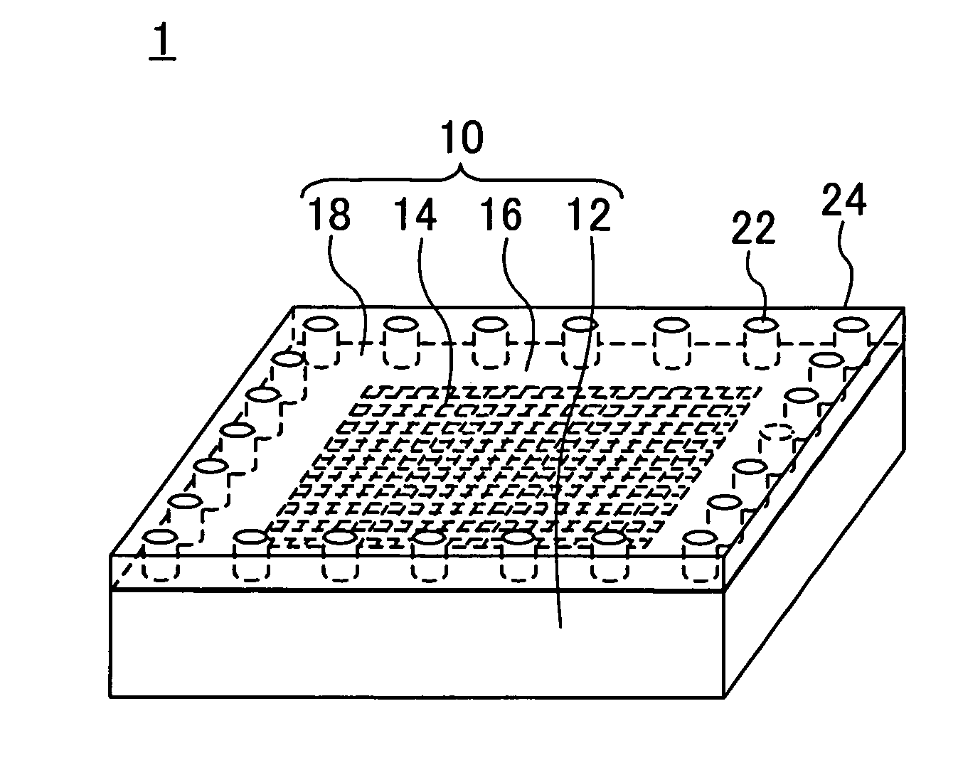
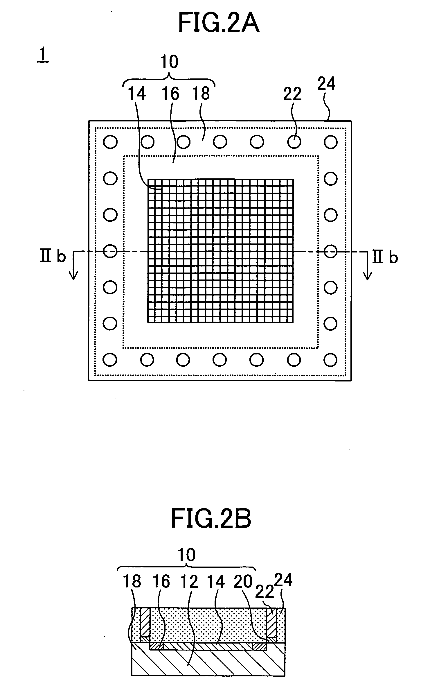
[0033]FIG. 1 is an oblique view schematically illustrating the entire structure of a semiconductor image sensor according to a first embodiment of the present invention. FIGS. 2A and 2B are a plan view and a cross-sectional view taken along the line IIb-IIb, respectively, each illustrating the semiconductor image sensor of this embodiment.

[0034] As shown in FIGS. 1 and 2, the semiconductor image sensor 1 of this embodiment includes a semiconductor imaging element 10, cylindrical electrodes 22, and a transparent resin layer 24 formed on the entire upper surface of the semiconductor imaging element 10.

[0035] The semiconductor imaging element 10 includes a semiconductor substrate 12, an imaging area 14 formed on the semiconductor substrate 12, a peripheral circuit area 16 surrounding the imaging area 14, and an electrode area 18 including electrode terminals 20 for establishing connection with an external circuit or circuits. The cylindrical electrodes 22 are formed on the electrode ...

second embodiment

[0064]FIGS. 5A and 5B are a plan view and a cross-sectional view taken along the line Vb-Vb, respectively, each schematically illustrating the entire structure of a semiconductor image sensor according to a second embodiment of the present invention. In FIGS. 5A and 5B, the same members as those in the semiconductor image sensor of the first embodiment shown in FIG. 2 are identified by the same reference numerals.

[0065] The semiconductor image sensor 2 of this embodiment differs from the semiconductor image sensor 1 of the first embodiment in that an antireflection film 32 is formed around the side face (i.e., the perimeter) of each electrode terminal 20 and of each cylindrical electrode 22. In the other respects, the semiconductor image sensor 2 of this embodiment has the same structure as the semiconductor image sensor 1 of the first embodiment, and the descriptions of the same members will be thus omitted herein.

[0066] The antireflection films 32, which are made of a material s...

third embodiment

[0073]FIGS. 7A and 7B are a plan view and a cross-sectional view taken along the line VIIb-VIIb, respectively, each schematically illustrating the entire structure of a semiconductor image sensor according to a third embodiment of the present invention.

[0074] As shown in FIGS. 7A and 7B, the semiconductor image sensor 3 of this embodiment includes a semiconductor imaging element 10, a transparent resin adhesive 38 applied onto the upper surface (the circuit-formation surface) of an imaging area 14 in the semiconductor imaging element 10, a transparent sheet 34 bonded to the upper surface of the imaging area 14 with the transparent resin adhesive 38, and an antireflection film 36 provided on the perimeter (i.e., the side faces) of the transparent sheet 34.

[0075] As in the first embodiment, the semiconductor imaging element 10 includes a semiconductor substrate 12, and the imaging area 14, a peripheral circuit area 16, and an electrode area 18 including electrode terminals 20, each ...


PUM


Abstract

A semiconductor image sensor includes: a semiconductor imaging element including an imaging area, a peripheral circuit area, and an electrode area; cylindrical electrodes provided on electrode terminals so as to be electrically connected with an external device; and a transparent resin layer provided on the upper surface of the semiconductor imaging element. The upper surface of each cylindrical electrode and the upper surface of the transparent resin layer are substantially of the same height.

Description

BACKGROUND OF THE INVENTION [0001] 1. Field of the Invention [0002] The present invention relates to semiconductor image sensors and methods for fabricating the same. [0003] 2. Description of the Related Art [0004] In recent years, as electronic devices have become smaller, thinner and lighter, there has been a growing demand for high-density packaging of semiconductor components. Because of this demand together with the high degree of integration achieved by the development of fine processing technology, semiconductor imaging elements, in particular, are being strongly required to shift from a conventional package type, in which a semiconductor imaging element is incorporated into a package, to another type, in which a semiconductor imaging element as a bare chip is directly mounted onto an electronic device. [0005] For example, Japanese Laid-Open Publication No. 2004-111792 discloses a semiconductor package, which includes no through-hole conductors so as to be reduced in thicknes...

Claims


Application Information

Patent Timeline
IPC IPC(8): H01L27/148H01L23/02H01L27/14H04N5/335H04N5/359H04N5/369
CPCH01L27/14618H01L27/14683H01L2924/0002H01L2924/00
Inventor MINAMIO, MASANORIFUKUDA, TOSHIYUKI
Owner COLLABO INNOVATIONS INC
Why Eureka
Try Eureka