SONOS memory cell having high-K dielectric

a memory cell and dielectric technology, applied in the field of nonvolatile memory, can solve the problems of net positive charge, reduced device threshold voltage, and process tend to damage the bottom oxide layer

Active Publication Date: 2007-02-08
LONGITUDE FLASH MEMORY SOLUTIONS LTD
View PDF31 Cites 28 Cited by
  • Summary
  • Abstract
  • Description
  • Claims
  • Application Information

AI Technical Summary

Problems solved by technology

This causes a net positive charge in the floating gate and reduces the threshold voltage of the device.
One potential problem associated with erasing the memory cell using HHI is that this process tends to damage the bottom oxide layer.

Method used


Image

  • SONOS memory cell having high-K dielectric
  • SONOS memory cell having high-K dielectric
  • SONOS memory cell having high-K dielectric

Examples


Embodiment Construction

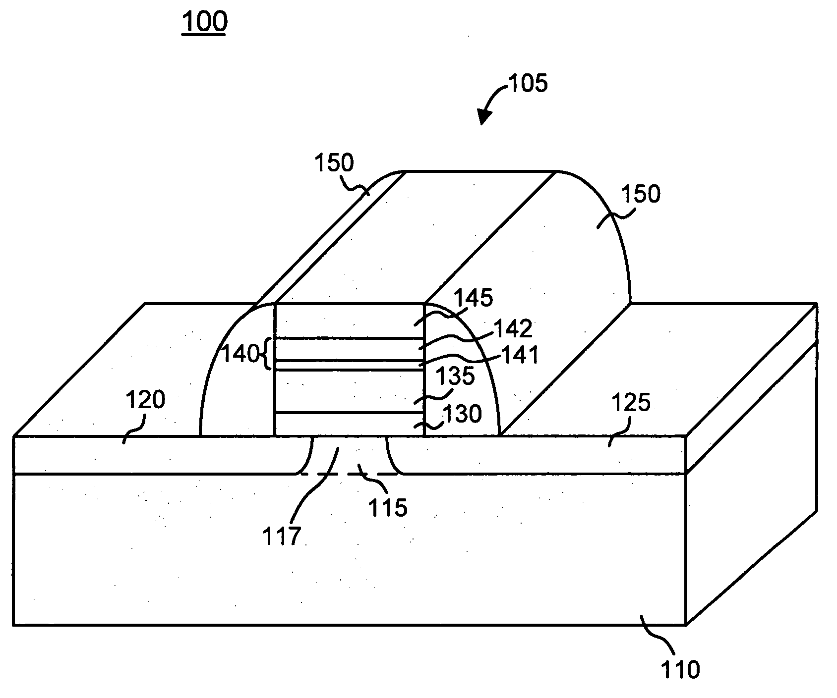
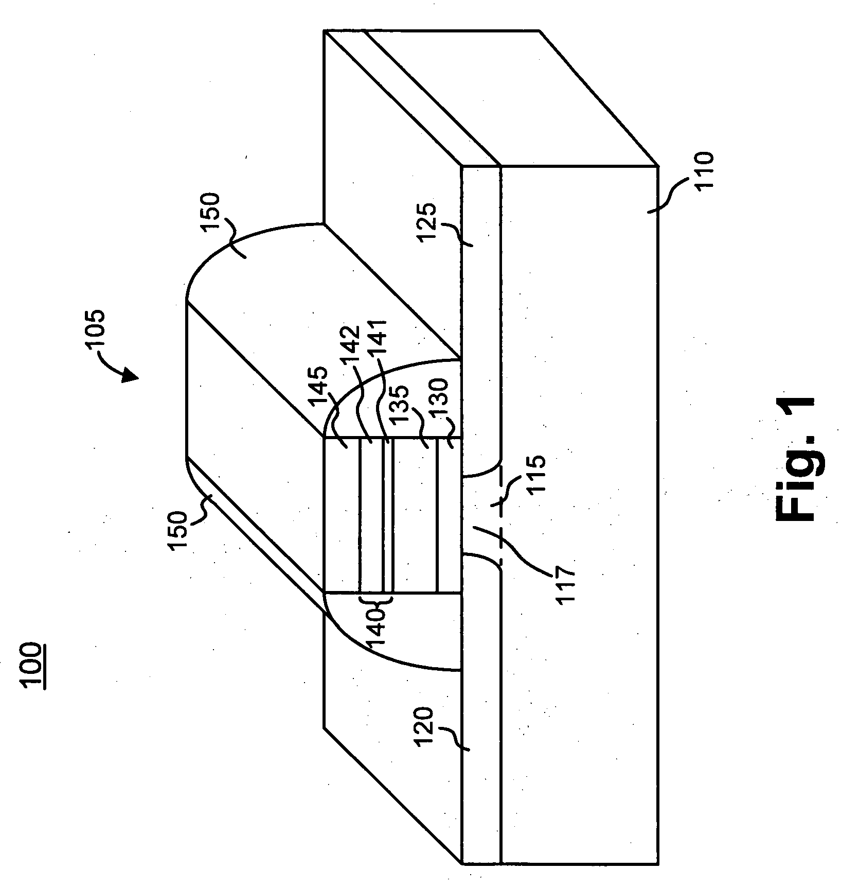
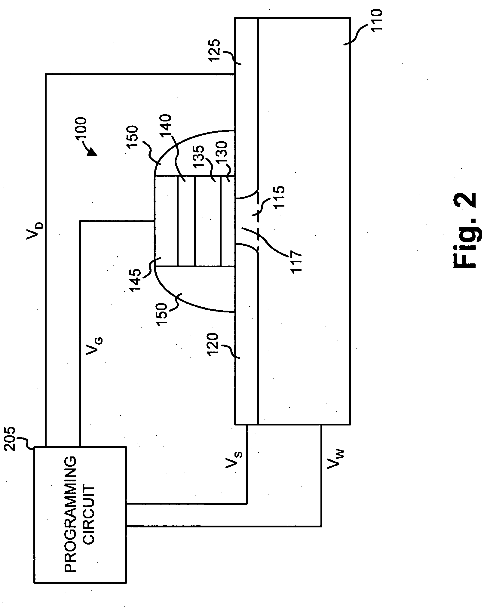
[0017] The following detailed description of the invention refers to the accompanying drawings. Also, the following detailed description does not limit the invention. Instead, the scope of the invention is defined by the appended claims and equivalents.

[0018] Techniques described below relate to a semiconductor memory device, a method of using the semiconductor memory device, and a method of making the semiconductor memory device. The semiconductor memory device may include an intergate dielectric layer of a high-K dielectric material interposed between the floating gate and the control gate. With this intergate high-K dielectric in place, the memory device may be programmed with hot electron injection and erased using Fowler-Nordheim tunneling. Although generally described herein as a single layer, it should be understood by those skilled in the art that the intergate dielectric layer of high-K dielectric material may be one or more layers of the same or different dielectric mater...


PUM


Abstract

A semiconductor memory device may include an intergate dielectric layer of a high-K dielectric material interposed between a floating gate and a control gate. With this intergate high-K dielectric in place, the memory device may be erased using Fowler-Nordheim tunneling.

Description

TECHNICAL FIELD [0001] Techniques described herein relate generally to non-volatile memory (NVM), and more specifically, to non-volatile memory devices having a silicon-oxide-nitride-oxide-silicon (SONOS) structure. BACKGROUND ART [0002] Conventional semiconductor memory devices may use a memory structure characterized by a vertical stack of a tunnel oxide (SiO2), a polysilicon floating gate over the tunnel oxide, an interlayer dielectric over the floating gate, and a control gate over the interlayer dielectric. The vertical stack may be formed on a crystalline silicon substrate. The substrate may include a channel region positioned below the vertical stack and a source and drain on opposing sides of the channel region. [0003] One particular type of memory cell structure is characterized by a vertical stack that includes an insulating oxide tunnel layer, a charge trapping nitride dielectric layer, an insulating top oxide layer, and a polysilicon control gate, all positioned on top o...

Claims


Application Information

Patent Timeline
Patent Type & Authority Applications(United States)
IPC IPC(8): H01L29/788H01L21/336
CPCH01L21/28282H01L29/792H01L29/513H01L29/4232H01L29/40117
Inventor ORIMOTO, TAKASHI WHITNEYJEON, JOONGSHIRAIWA, HIDEHIKOCHAN, SIMON S.SACHAR, HARPREET K.
Owner LONGITUDE FLASH MEMORY SOLUTIONS LTD
Why Eureka
Try Eureka