Display device and manufacturing method of display device

a display device and manufacturing method technology, applied in the direction of semiconductor devices, organic semiconductor devices, electrical devices, etc., can solve the problems of low reliability, limited practical application, and significant degradation of luminescence properties such as luminance or evenness, and achieve high reliability of display devices, high resolution, and high performance display

Inactive Publication Date: 2007-02-15
SEMICON ENERGY LAB CO LTD
View PDF24 Cites 24 Cited by
  • Summary
  • Abstract
  • Description
  • Claims
  • Application Information

AI Technical Summary

Benefits of technology

[0014] By applying the present invention, a highly reliable display device can be manufactured.

Problems solved by technology

An electroluminescence element (hereinafter, also referred to as an EL element) has a problem in that luminescence properties such as luminance or evenness

Method used


Image

  • Display device and manufacturing method of display device
  • Display device and manufacturing method of display device
  • Display device and manufacturing method of display device

Examples


embodiment mode 1

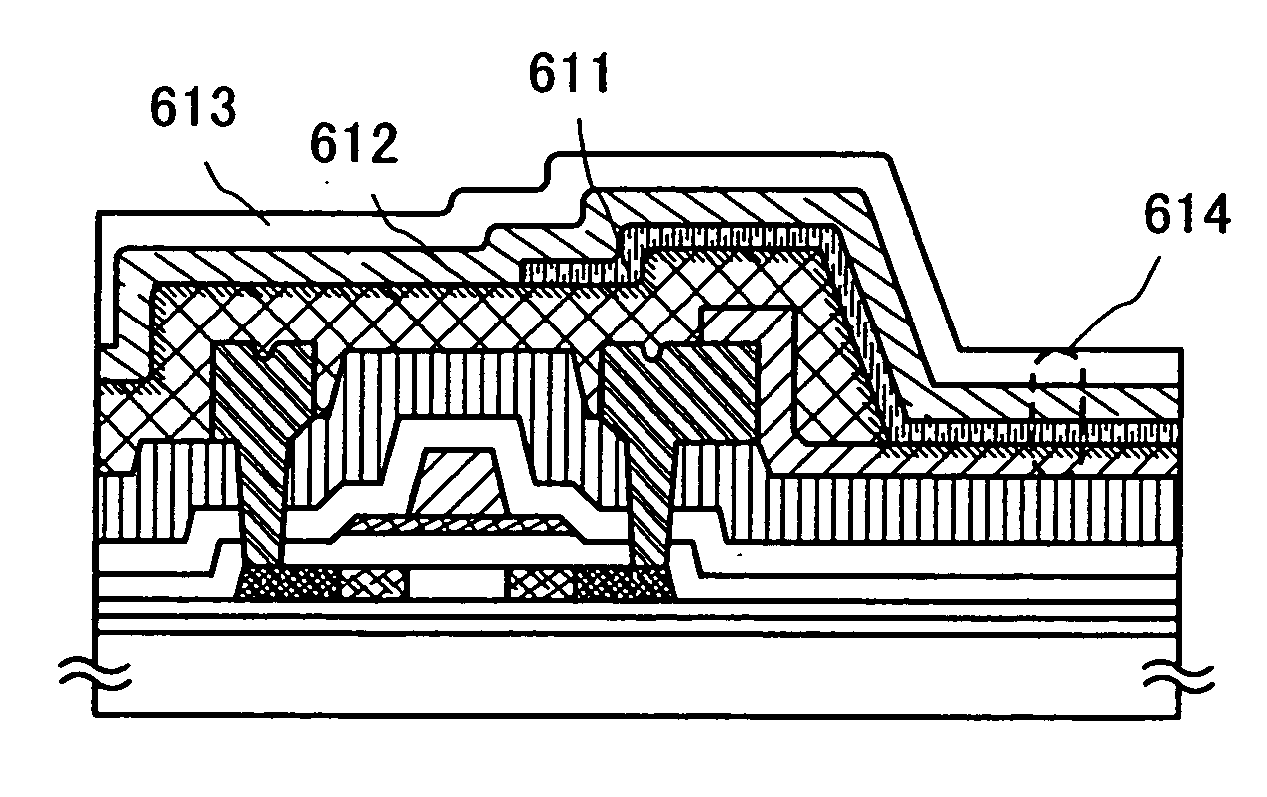
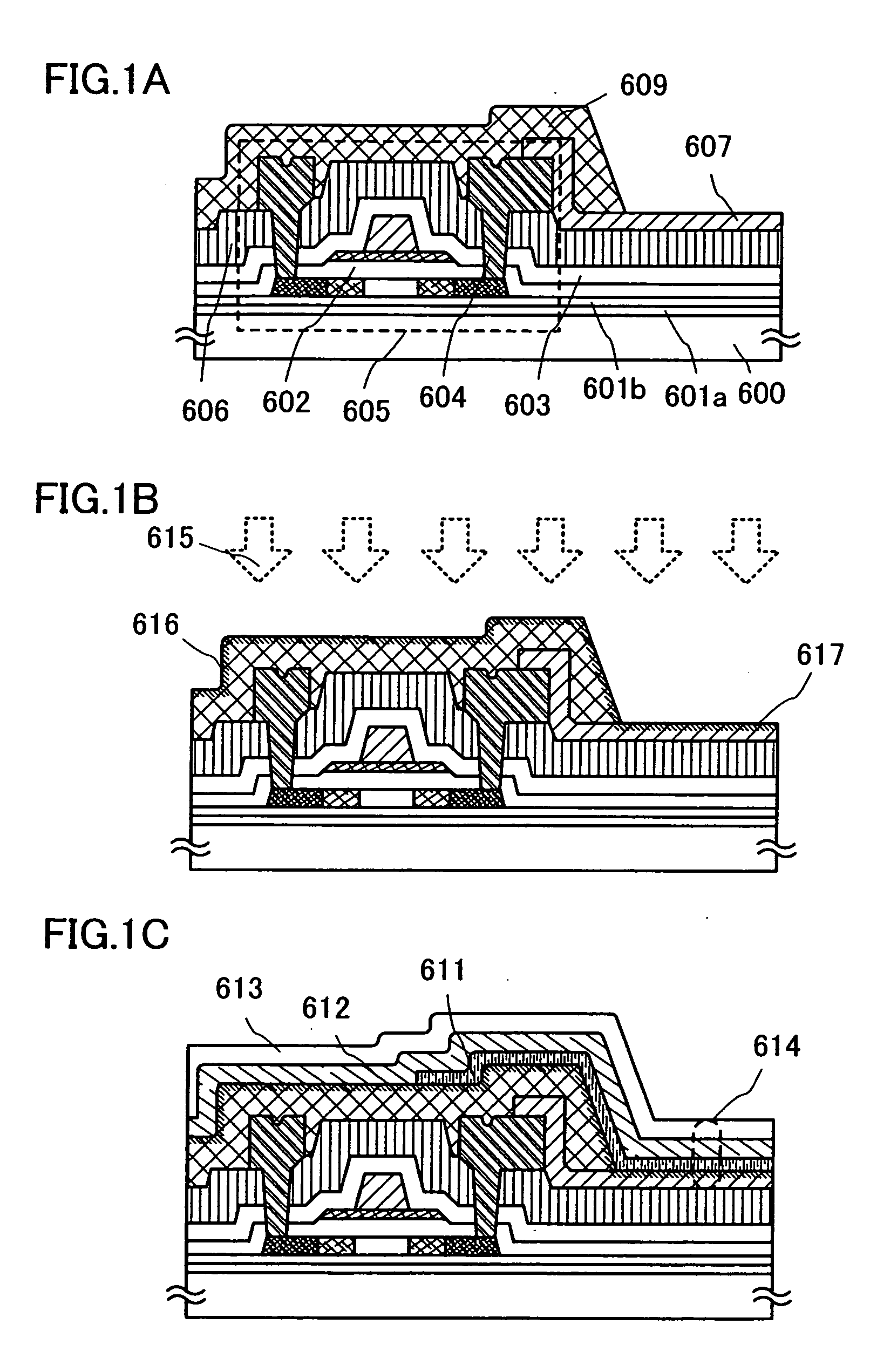
[0046] A manufacturing method of a display device in this embodiment mode will be explained with reference to FIGS. 1A to 1C.

[0047] Over a substrate 600, base films 601a and 601b, a thin film transistor 605, a gate insulating layer 602, insulating layers 603 and 606, a first electrode layer 607, and an insulating layer 609 serving as a partition (also referred to as a barrier or the like) are formed (see FIG. 1A). The thin film transistor 605 includes a semiconductor layer having impurity regions each serving as source and drain regions, the gate insulating layer 602, gate electrode layers in a two-layer stacked structure, and source and drain electrode layers 604. The source or drain electrode layer is electrically connected to the impurity region of the semiconductor layer and the first electrode layer 607 by being in contact therewith.

[0048] In this embodiment mode, regions of the impurity regions, which overlap with the gate electrode layers with the gate insulating layer inte...

embodiment mode 2

[0070] A manufacturing method of a display device in this embodiment mode will be explained in detail with reference to FIGS. 27A to 27C. This embodiment mode shows an example in which a structure of an insulating layer to be a partition is different from the one in Embodiment Mode 1. Thus, repeated explanations of the same portions or portions having the same function will be omitted.

[0071] Over a substrate 620, a base film 621a, a base film 621b, a thin film transistor 625, a gate insulating layer 622, insulating layers 623 and 626, a first electrode layer 627, a first insulating layer 628 and a second insulating layer 629 each serving as a partition (also referred to as a barrier or the like) are formed (see FIG. 27A). The thin film transistor 625 includes a semiconductor layer having impurity regions each serving as source and drain regions, the gate insulating layer 622, gate electrode layers in a two-layer stacked structure, and source and drain electrode layers 624. The sour...

embodiment mode 3

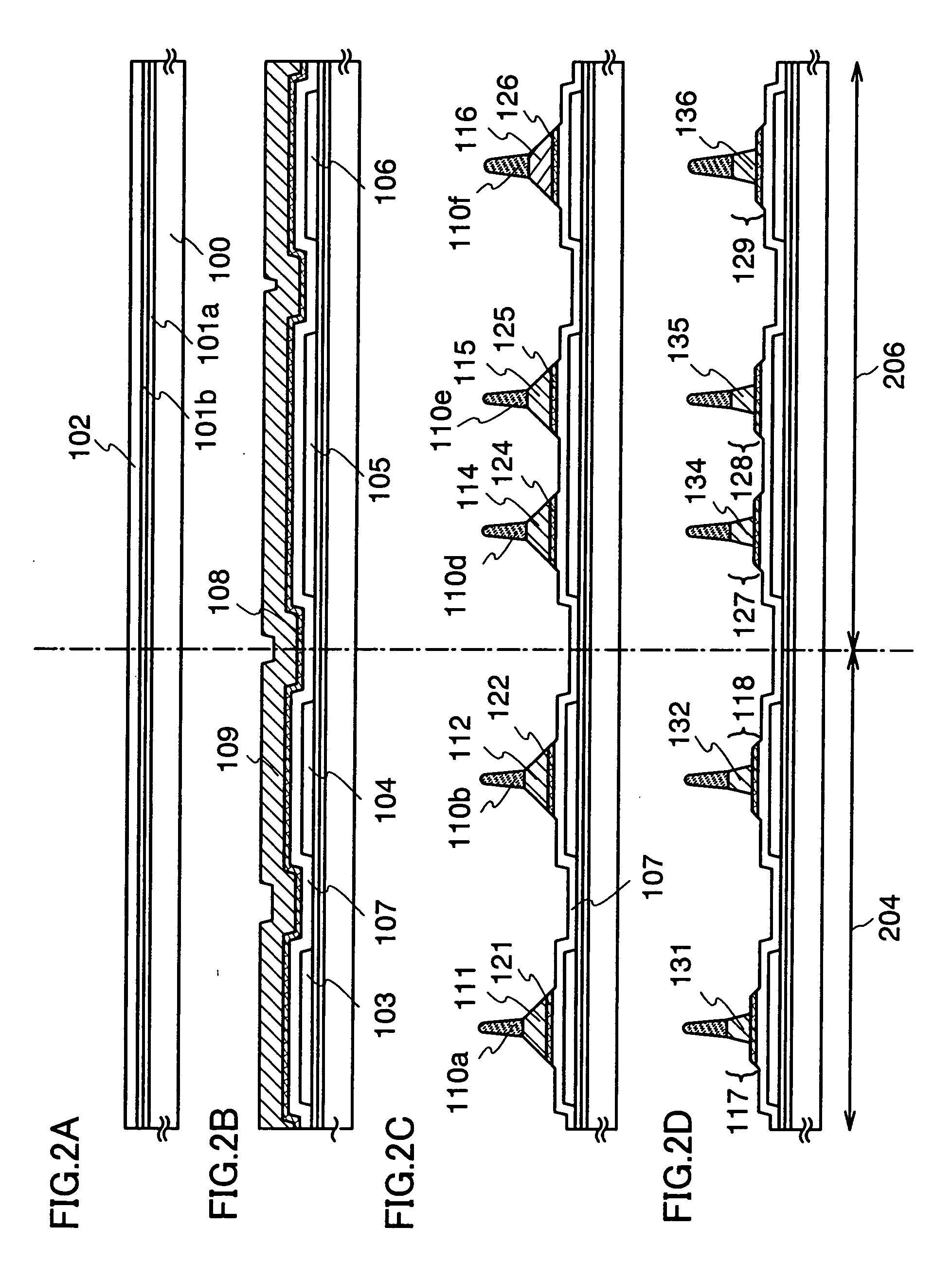
[0091] A manufacturing method of a display device in this embodiment mode will be explained in detail with reference to FIGS. 2A to 2D, FIGS. 3A to 3C, FIGS. 4A to 4C, FIGS. 5A to 5C, FIGS. 6A to 6C, FIGS. 7A and 7B, FIGS. 8A to 8C, FIG. 9, FIG. 10, FIGS. 16A to 16C, and FIGS. 17A and 17B.

[0092]FIG. 16A is a top view showing a structure of a display panel according to the present invention, which includes a pixel portion 2701 in which pixels 2702 are arranged in matrix, a scanning line input terminal 2703, and a signal line input terminal 2704 over a substrate 2700 having an insulating surface. The number of pixels may be set depending on various standards, for example, 1024×768×3 (RGB) in a case of a full color display using RGB which is XGA, 1600×1200×3 (RGB) in a case of a full color display using RGB which is UXGA, and 1920×1080×3 (RGB) in a case of a full color display using RGB with the use for a full spec high vision display.

[0093] The pixels 2702 are arranged in matrix by ...


PUM


Abstract

According to one feature of the present invention, a display device is manufactured according to the steps of forming a semiconductor layer; forming a gate insulating layer over the semiconductor layer; forming a gate electrode layer over the gate insulating layer; forming source and drain electrode layers in contact with the semiconductor layer; forming a first electrode layer electrically connected to the source or drain electrode layer; forming an inorganic insulating layer over part of the first electrode layer, the gate electrode layer, the source electrode layer, and the drain electrode layer; subjecting the inorganic insulating layer and the first electrode layer to plasma treatment; forming an electroluminescent layer over the inorganic insulating layer and the first electrode layer which are subjected to plasma treatment; and forming a second electrode layer over the electroluminescent layer.

Description

BACKGROUND OF THE INVENTION [0001] 1. Field of the Invention [0002] The present invention relates to a display device and a manufacturing method of a display device. [0003] 2. Description of the Related Art [0004] In a display device provided with an electroluminescence (hereinafter, also referred to as EL) element, a color light-emitting element that emits color light is used to perform full color display. Forming a light-emitting material of each color over an electrode in a minute pattern is one of important elements to form a color light-emitting element. [0005] The light-emitting element is isolated in every pixel, which is single or plural, by an insulating layer. As the insulating layer like this that isolates between pixels, an inorganic insulating material has been used (for example, see Reference 1: Japanese Patent Application Laid-Open No. 2003-288994). [0006] An electroluminescence element (hereinafter, also referred to as an EL element) has a problem in that luminescenc...

Claims


Application Information

Patent Timeline
IPC IPC(8): H01L21/336
CPCH01L27/3246H01L27/3258H01L51/5206H01L51/5237H01L51/56H01L2251/5315H01L2251/5323H01L51/5221H10K59/122H10K59/123H10K59/124H10K59/1213H10K50/81H10K50/828H10K50/846H10K50/8426H10K2102/3031H10K2102/3026H10K71/00
Inventor SUZAWA, HIDEOMIYAMAZAKI, SHUNPEI
Owner SEMICON ENERGY LAB CO LTD
Why Eureka
Try Eureka