Dual trench isolation for CMOS with hybrid orientations

Inactive Publication Date: 2007-02-22
GLOBALFOUNDRIES INC
View PDF2 Cites 35 Cited by
  • Summary
  • Abstract
  • Description
  • Claims
  • Application Information

AI Technical Summary

Benefits of technology

[0027] In accordance with the present invention, the method of the present invention further comprises forming first semiconductor devices having a first polarity on one of said coplanar surfaces of different crystallographic orientation and forming second semiconductor devices having a second polarity on the other coplanar surface. Thus, nFETs can be built into one of the crystallographic surfaces, while pFETs can be built into the other crystallographic surface. In accordance with the present invention, the pFETs are built into a crystal surface

Problems solved by technology

To compensate for this discrepancy, pFETs are typically designed with larger widths in order to balance pull-up currents against the nFET pull-down currents and achieve uniform circuit switching. pFETs having larger widths are undesirable since they take up a significant amount of chip area.
Unfortunately, electron mobilities on (110) Si surfaces are significantly degraded compared to (100) Si surfaces.
As can be dedu

Method used


Image

  • Dual trench isolation for CMOS with hybrid orientations
  • Dual trench isolation for CMOS with hybrid orientations
  • Dual trench isolation for CMOS with hybrid orientations

Examples


Example

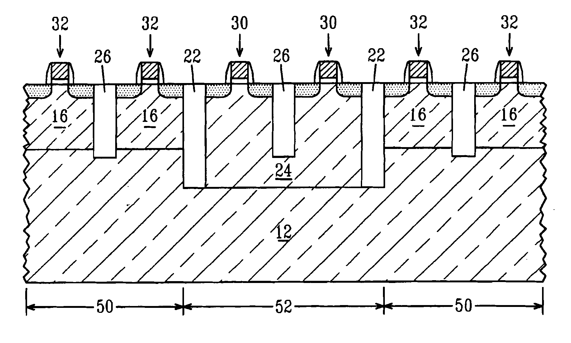
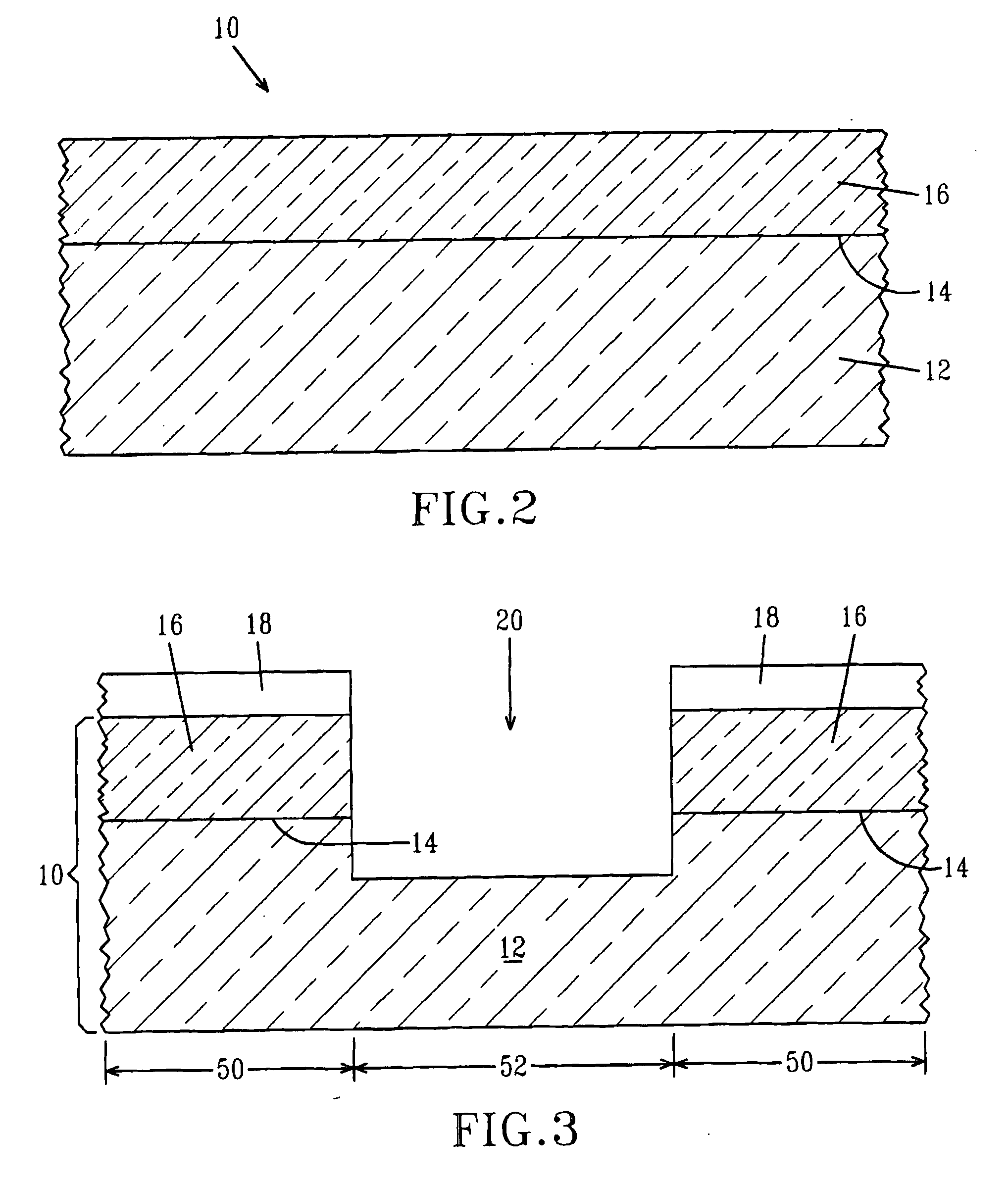
[0032] The present invention, which relates to dual trench isolation for CMOS devices located on a hybrid oriented substrate, will now be described in greater detail by referring to the drawings that accompany the present application. It is noted that the drawings of the present invention are provided for illustrative purposes and thus they are not drawn to scale.

[0033] Reference is first made to FIG. 2 which shows an initial hybrid substrate 10 having different crystal orientations that can be employed in the present invention. Specifically, the hybrid substrate 10 includes a first (i.e., bottom) semiconductor layer 12 and a second (i.e., top) semiconductor layer 16 having a bonding interface 14 located therebetween. In accordance with the present invention, the first semiconductor layer 12 has a first crystallographic orientation and the second semiconductor layer 16 has a second crystallographic orientation which differs from that of the first crystallographic orientation.

[0034...


PUM


Abstract

The present invention provides a semiconductor structure in which different types of devices are located upon a specific crystal orientation of a hybrid substrate that enhances the performance of each type of device. In the semiconductor structure of the present invention, a dual trench isolation scheme is employed whereby a first trench isolation region of a first depth isolates devices of different polarity from each other, while second trench isolation regions of a second depth, which is shallower than the first depth, are used to isolate devices of the same polarity from each other. The present invention further provides a dual trench semiconductor structure in which pFETs are located on a (110) crystallographic plane, while nFETs are located on a (100) crystallographic plane. In accordance with the present invention, the devices of different polarity, i.e., nFETs and pFETs, are bulk-like devices.

Description

RELATED APPLICATIONS [0001] This application is related to co-pending and co-assigned U.S. patent application Ser. No. 10 / 799,380, filed Mar. 12, 2004, Ser. No. 10 / 696,634, filed Oct. 29, 2003, and Ser. No. 10 / 250,241, filed Jun. 23, 2003, the entire contents of each application are incorporated herein by reference.FIELD OF THE INVENTION [0002] The present invention relates to high-performance metal oxide semiconductor field effect transistors (MOSFETs) for digital and analog applications, and more particular to MOSFETs utilizing carrier mobility enhancement from surface orientation in which a dual trench isolation design is employed. Specifically, a first trench isolation region having a first depth is used to isolate nFETs from pFETs, while second trench isolation regions having a second depth, which is shallower than the first depth, are used to isolate nFETs from nFETs and pFETs from pFETs. BACKGROUND OF THE INVENTION [0003] In present semiconductor technology, complementary met...

Claims


Application Information

Patent Timeline
IPC IPC(8): H01L29/04H01L21/76
CPCH01L21/76229
Inventor CHAN, VICTORIEONG, MEIKEIRENGARAJAN, RAJESHREZNICEK, ALEXANDERSUNG, CHUN-YUNGYANG, MIN
Owner GLOBALFOUNDRIES INC
Why Eureka
Try Eureka